Oscillation Circuit & Examination Method
| contents | |
| 1 | |
| 2 | |
| 3 | |
| 4 | |
| 5 | |
| 6 | |
| 7 |
1. Oscillation circuit
The crystal resonator is a passive component, and is therefore affected by the power voltage, ambient temperature, circuit configuration, circuit constant and substrate wiring pattern, etc. There can be classified roughly into 2 types of operation, normal and abnormal. In the design of the oscillation circuit, therefore, to ensure oscillation of crystal resonator and keeping it stable should be considered first. After those points are confirmed, accuracy of frequency, frequency pullability, modulation level, start-up time and others should be considered as the next step.
2. Roles of components & reference values
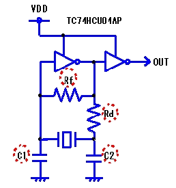 Fig. 1 |
In the design of the oscillation circuit, it is necessary to understand the role of individual components. Referencing to C-MOS IC (Toshiba: 74HCU04AP) based oscillation circuit (Fig.1), the roles are discribed in Table 1.
When the feedback resistor (Rf) is not mounted in the oscillation circuit, as shown in Table 1, the resonator does not start oscillation even if power is applied to the oscillation circuit. Unless a resistor of appropriate value is connected, oscillation may not start in the desired mode of the crystal resonator but undesired overtone or fundamental oscillation may start instead.
In the case of the fundamental resonator (MHz band) feedback resistance is usually 1 MΩ. In the case of the overtone resonator (MHz band), depending on IC and frequency characteristics, it is in the range of several kΩ- tens of kΩ. In the case of tuning fork type resonators (kHz band), it is necessary to connect a resistor of 10 MΩ or more.
| Parts No. | Parts name | Roles |
|---|---|---|
| Rf | Feedback resistance | Feedback current and signal from output to input of invertor in the oscillation circuit. Its value changes depending order of oscillation. |
| Rd | Dumping resistance | Limits the current that flows into resonator, adjusts the negative resistance and drive level, prevents abnormal oscillation of resonator and suppresses frequency fluctuations. |
| C1,C2 | External capacitors | Adjusts the negative resistance, drive level and oscillating frequency. Also sets any given load capacity. |
Appropriate values of dumping resistor (Rd) depend on the type of resonator, frequency band and the value of the external capacitor (C1, C2). The most optimized values are determined after measuring the characteristics of the oscillation circuit (including negative resistance, drive level and so on). Reference values for the AT cut resonator (MHz band) are in the range of several hundred Ω-several kΩ. For tuning fork type resonators (kHz band) the reference values are in the range of 100 kΩ - several hundred kΩ.
Appropriate values of external capacitors are in the range of 3 pF - 33 pF depending on the type of resonator, frequency band, value of dumping resistors and the order of oscillation.
3. Methods of examining oscillation circuit
Measurement of oscillating frequency
It is essential to measure correct values, as far as possible, of the oscillating frequency of the resonator mounted on the circuit, using correct methods. In the measurement of oscillating frequency, probes and frequency counters are usually used and the most important point is to minimize influence of measuring tools for measurement.
There are three methods of measuring frequencies, as shown in the following figures (Fig. 2, 3 and 4). The most accurate method of measurement is to use a spectrum analyzer having capability to measure without contacting the oscillation circuit.
In Fig.2, probes do not affect frequency because the frequency output from the buffer invertor is measured.In Fig.3, probes do not affect frequency because the buffer output frequency (1/1, 1/2, etc.) in IC is measured.
In Fig. 4, in the case of no buffer output from the IC, to minimize influence of probes, a capacitor smaller than 3pF is inserted between the output pin of IC (XTAL OUT) and the probe. However, using this method, the output waveform may be smaller and may not be measured with frequency counter due to sensitivity of frequency counter even though it can be measured with oscilloscope. In that case, use an amplifier for measurement.
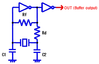 Fig. 2 |
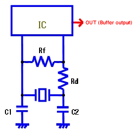 Fig. 3 |
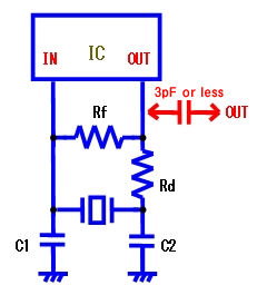 Fig. 4 |
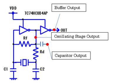 Fig. 5 |
In addition, oscillating frequency is different by the measurement points.
①Measuring the buffer output
②Measuring the oscillating stage output
③Measuring the oscillating stage output via a capacitor
Fig. 5shows above 1-3 measurement points and the measured oscillating frequencies except the buffer output are lower by the influence of the probe.
4. Measurement of negative resistance
This is the measurement used to determine the margin of oscillation of the oscillation circuit, and is used to predict the stability of oscillation from obtained values.
As shown in Fig. 6, connect the resistor (R) in series to the resonator and increase the value gradually. The resonator will then stop oscillating at a certain value of resistance. This resistance value just before the resonator stops oscillation is the value of negative resistance.
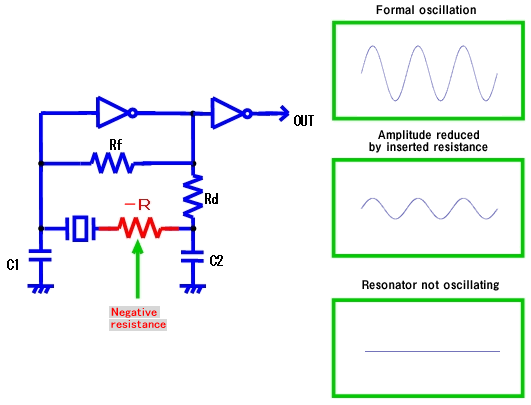 Fig. 6 |
【Cautions:】
-
-
- Check oscillation waveform with an oscilloscope at the measurement point.
- Check the minimum value of negative resistance in the operating voltage range.
- Check negative resistance by changing temperature for the measurement result at room temperature.
(Use dryers, quenching agents, temperature controlled ovens, etc. according to the operating temperature range.) - Negative resistance 5 times greater than maximum crystal series resistance is recommended.
-
*These reference values are subject to change without prior notice.
5. Measurement of drive levels
In the oscillation circuit used, measure the power consumed by an operating resonator. As shown in Fig. 7, measure the current (i) that flows into the resonator by using a current probe.
Other measurements may be available. In the method using a probe contacting the oscillation circuit, however, correct value cannot be obtained because current flows into the GND from the probe.
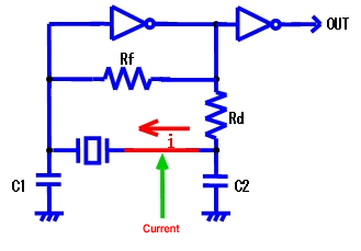 Fig. 7 |
| Calculation formula |
|---|
| DL(drive level:W)=i2×R1 i(A):Current (effective value) R1(Ω):Serial resistance of resonator |
【Caution:】
Allowable Max. drive level of resonator depends on the size of resonator and oscillation mode. Please contact us for details.
6.Check of abnormal oscillation
In the oscillation circuit, check for the possibility of resonator oscillation with undesired oscillation mode.
Simple method of checking
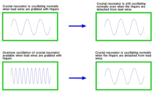
When the oscillation mode of the resonator is fundamental, as shown in Fig. 9, abnormal oscillation can be tested by grabbing the lead (2 pcs) of the resonator with slightly wet fingers and detaching the fingers while turning the power from OFF to ON. If the 3rd overtone oscillation is not observed in oscilloscope, there is no possibility of abnormal oscillation. On the other hand, if the 3rd overtone oscillation is observed in oscilloscope when the fingers are detached, there is a possibility of abnormal oscillation.
Checking by wet fingers is to form a small resistance between resonator terminals and reduce Rf as shown in the circuit diagram in Fig. 8 to allow oscillation with high frequency band.
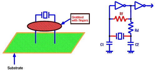 Fig. 8 |
| Normal: |
 |
| Abnormal: |
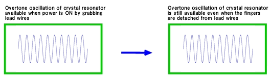 Fig. 9 |
7. Nonconforming conditions caused by oscillation circuit & sample countermeasures
In the design of the crystal oscillation circuit, various nonconforming conditions may occur.
For example;
-
-
- Frequency cannot be within the required range. (Although application requires precise frequency stability.)
- Frequency cannot be adjusted. (Although frequency tunable circuit.)
- Oscillation with 1/3 or 3 times of nominal frequency
- Start-up time of oscillation is significantly delayed.
- Resonator does not oscillate or Start-up time of oscillation is long.
-
To suppress such symptoms, therefore, it is essential, at least, to examine the basic items of oscillation circuit described above.
If, here, the specification of resonator need not be changed to solve nonconforming conditions, it is comparatively easy to implement countermeasures in the circuit side (See Table-2).
However, many characteristics of the oscillation circuit may not be met even if the conforming conditions are improved and other nonconforming conditions could occur. Therefore, the circuit should be examined by crystal supplier. Also, if you cannot solve the problem even implementing the sample countermeasures below, please contact our sales representative, we will examine the circuit to try to solve the problem.
Table-2
| Nonconforming condition | Cause | Example countermeasure |
|---|---|---|
| Frequency is deviated | Load capacity of resonator is not aligned to that of oscillation circuit. | Change the circuit constant (C1,C2). |
| Change the load capacity of resonator. | ||
| Frequency cannot be adjusted | Frequency pullability by trimmer capacitor is insufficient. | Reduce the capacity of trimmer capacitor or fixed capacitor. |
| Oscillation with 3 times of nominal frequency | Circuit constant is not aligned to the oscillation order of resonator. | Increase the value of feedback resistance (Rf). |
| Insert control resistance (Rd). | ||
| Increase the value of outfit capacitor (C1, C2). |
||
| Oscillation with 1/3 of nominal frequency | Circuit constant is not aligned to the oscillation order of resonator. | Decrease the value of feedback resistance (Rf). |
| Decrease the value of control resistance (Rd). | ||
| Decrease the value of outfit capacitor (C1, C2). |
||
| No oscillating | Circuit negative resistance with is too low. | Decrease the value of control resistance (Rd). |
| Long start-up time | Decrease the value of outfit capacitor (C1, C2). |