Advantages of embedding parts into ICs
Demand for evolution of electronic parts
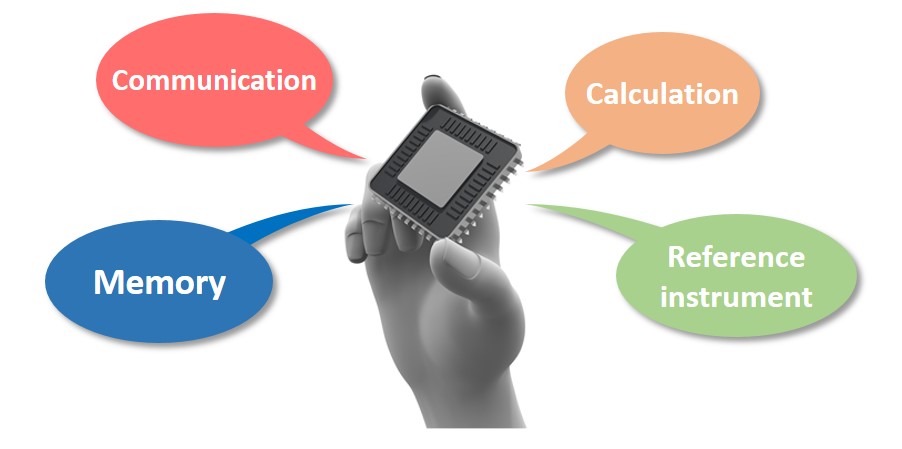
In recent years, all electronic devices, including smartphones, have become smaller and more functional. As a result, the number of electronic parts incorporated has increased. A smartphone contains more than 1,500 electronic parts. Even more electronic parts are used in a vehicle.
Notably, miniaturization of mobile devices is required for user friendliness. However, an increase in the number of parts makes it difficult to reduce the size of mobile devices. Thus, there is demand for further miniaturization of internal electronic parts. To prevent the number of parts from increasing, the functionality of a single part must be enhanced to be multifunctional.
To this end, packaging technologies for electronic parts must be advanced. A technology has been developed for high-density implementation of various electronic parts in a single package. This technology makes it possible to embed multiple electronic parts in a single IC chip.
What are specific advantages of embedding parts into a single IC chip?
Advantages of embedding parts into ICs
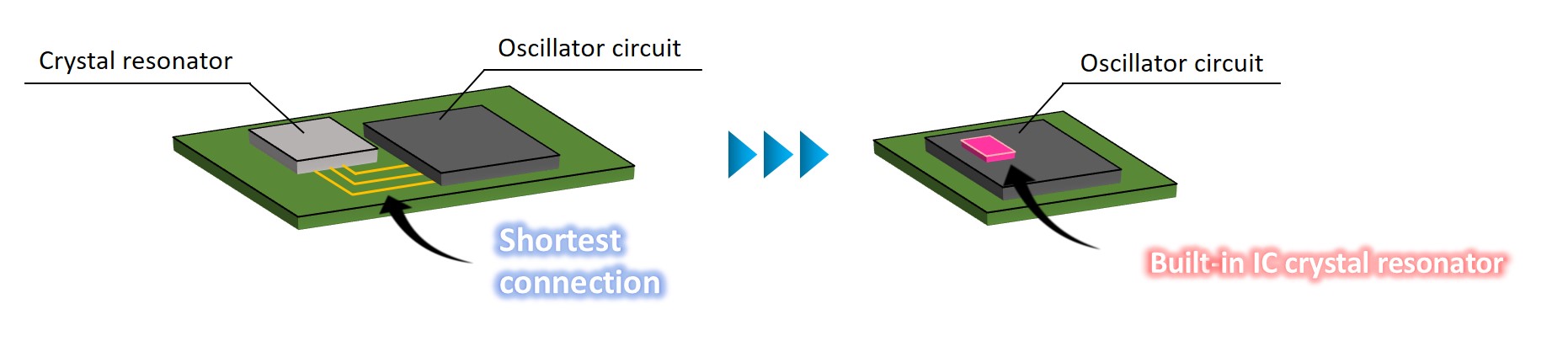
In the case of a smartphone, the printed circuit board can be miniaturized by embedding electronic parts into a single IC chip. The usage time can be extended by placing a large battery in the freed-up space.
A crystal resonator is connected to an oscillator circuit IC. Longer wiring increases wasted power, resulting in lower performance. Higher frequencies generate noise and affect surrounding devices. Thus, wiring to connect with an IC must be minimized. A crystal resonator should be miniaturized and installed in close proximity to an oscillator circuit IC. Ideally, it should be embedded in an IC. However, crystal resonators require an internal space larger than that of other parts. There were limitations to miniaturization and reduction in thickness.
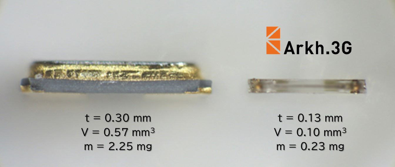
Arkh series embeddable in ICs
The Arkh series crystal resonators, which are our key products, solve the problem.
WLP (wafer-level packaging) technology is used for the Arkh series to bond crystal wafers together. The technology secures minimal space to allow a crystal blank to physically resonate, which was difficult to achieve using conventional ceramic packaging. The size is smaller than that of conventional products, and the thickness is half or less.
As a result, the products can be mounted into even narrower gaps. They are suitable for high-density surface mounting. Manufactured by photolithography technology, the Arkh series products have superb high-frequency performance and are suitable for applications in high-speed, large-capacity communication, which must meet high-frequency requirements in recent years.