To offer new value of quartz crystal devices
Trends in parts used in mobile devices
Information devices, such as smartphones and smartwatches, and wearable devices, such as wireless earphones and smart glasses, have come into popular use. These devices have enabled high-speed, large-capacity communication and high-speed processing, making our lives more convenient. In addition, the size of batteries installed in these devices has increased to offer a long battery life. While the size of batteries has increased, the size and thickness of other parts have been reduced to meet higher precision requirements. The size (volume) of quartz crystal devices has been reduced to about one eighth during the past 20 years. Today, these devices are smaller than a grain of rice. However, quartz crystal devices are still large compared to other parts. There has been a growing need for further miniaturization.
Issues in miniaturizing quartz crystal devices
Regarding the basic structure of a quartz crystal device, a quartz crystal blank is fixed on a ceramic package using an adhesive and is sealed using a metallic lid. Previously, miniaturization was achieved by reducing the size and thickness of the package and lid and reducing the size of the quartz crystal blank that was placed inside. However, the thinner the package and lid, the more fragile and difficult to handle they become, resulting in higher difficulties in processing and assembly. The following techniques are required to make quartz crystal devices even smaller and thinner.
▶ The materials used must be thin and durable and enable high-precision processing
▶ The gap between the quartz crystal blank and the package or lid must be minimized

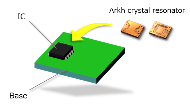
Smallest and thinnest quartz crystal devices in the world
The Arkh series, which represents our key products, uses durable quartz crystals, which enable high-precision processing, as packages, making it possible to achieve integrated forming with the quartz crystal blank inside and minimize the internal gap. The wafer-level packaging (WLP) method is also used to enable assembly of many tiny quartz crystal devices at a time, using a large wafer, making handling easier and keeping manufacturing costs low. The series also supports high-density surface mounting, such as System In Package (SIP), that realizes high-functionality devices. Previously, the thickness of the thinnest quartz crystal device was 300 μm. However, the Arkh.3G, a part of the Arkh series, is 130 μm in thickness, which is less than half that of conventional products, enabling installation of quartz crystal devices in locations that were considered difficult before. The potential of the Arkh series continues to expand.