Challenge of achieving seven times the output per unit area
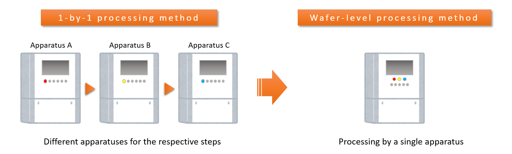
Limitations of the 1-by-1 processing method
If the number of plants and pieces of equipment is increased to expand the production capacity in response to ever-increasing demand, the environmental impact will increase, making it difficult to achieve both “stable supply” and “environmental initiatives.”
It is necessary to improve productivity. In the conventional 1-by-1 processing method (in which products are processed one by one), productivity can be improved by reducing the takt time (i.e., time required to process a single product). However, recent products that are needed in the market require further miniaturization and higher accuracy in the manufacturing process. There are limitations to reduction in takt time and production by the 1-by-1 processing method. That is, improvement in productivity requires products and production lines based on a new design concept.
A shift from the 1-by-1 processing method to the wafer-level processing method
Against this backdrop, we aim to improve productivity by shifting from the conventional 1-by-1 processing method to the wafer-level processing method.
In the wafer-level processing method, processing in each step can be performed in a batch, making it possible to simplify the steps and reduce the scale of commonized equipment. For example, in the 1-by-1 processing method, different apparatuses are used in respective steps until a quartz crystal is mounted and sealed on a ceramic package using adhesive. In the wafer-level processing method, these steps can be processed using the same equipment. However, a fundamental review of the product design concept was also required to realize the wafer-level processing method. The review led to the development of the Arkh series products, which are our original key products.
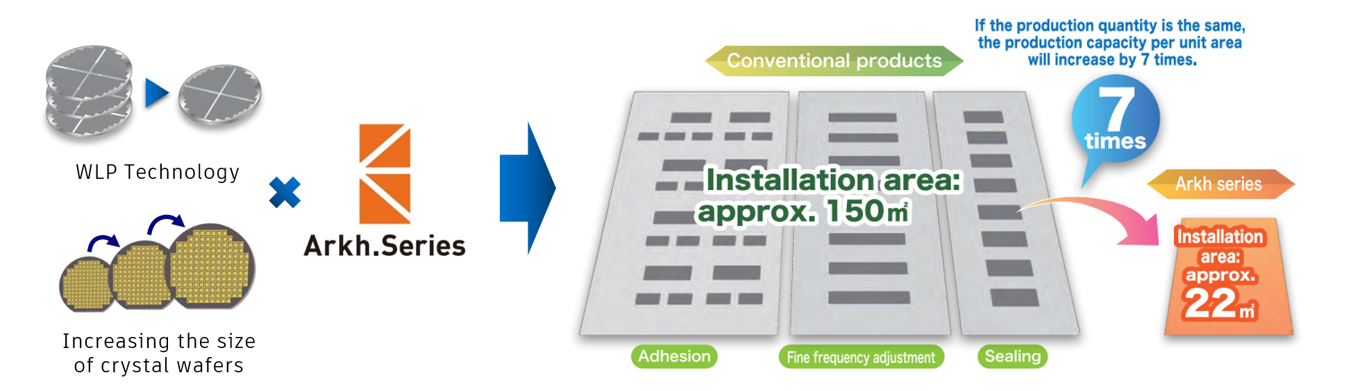
To achieve seven-times output per unit area
Unlike a conventional structure in which a quartz crystal element is held in a ceramic package using a conductive adhesive, the Arkh series adopts wafer-level packaging (WLP) technology that allows three crystal wafers to be bonded together. For this reason, unlike conventional products, the Arkh series products do not need to be transferred one by one for each process, so the number of pieces of equipment can be reduced and the equipment installation area can be significantly reduced. Furthermore, in the 1-by-1 processing method, crystal blanks are mounted on ceramic packages one by one for assembly. Thus, the production capacity depends on the capacity of the assembly equipment. Meanwhile, WLP technology enables assembly on wafers. Thus, the number of quartz crystal devices that can be manufactured in a single assembly process depends on the wafer size. In other words, using larger crystal wafers can increase the output per unit area. We have realized six-inch quartz crystal wafers, which are the largest in the world. We have also been working to achieve even larger eight-inch wafers.
Previously, productivity was enhanced with the aim of cutting costs and expanding the production scale. Recently, the aim has shifted to labor saving and environmental initiatives. By reducing the equipment installation area and using WLP technology, we will increase the production capacity per unit area to seven times the current level. While ensuring a stable supply without expanding plants or the equipment installation area, we are taking on the challenge of reducing CO2 emissions.