Technology to process synthetic quartz crystals -Aiming to further improve the processing accuracy-
The previous story explained the workflow to process 6-inch wafers from synthetic quartz crystals. This story takes a closer look at the lapping process and introduces new surface processing technology.
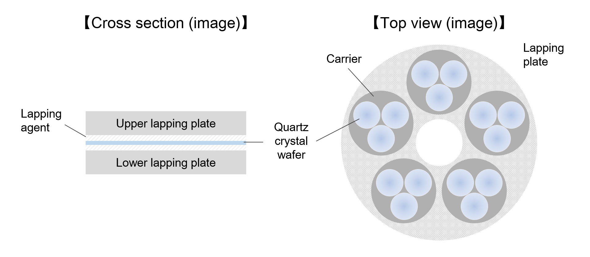
About the lapping process
In the lapping process, a quartz crystal wafer is rubbed against a lapping plate using a lapping agent to smooth the wafer.
Wafer flatness is an important factor in the lapping process. Why does wafer flatness matter? The frequency value of the reference signal is determined by the thickness of a quartz crystal. If a wafer with thickness variation is processed, it takes time to make adjustments to the required frequency, resulting in decreased productivity.
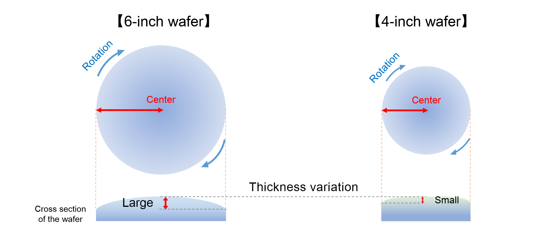
The figure above shows the image of the lapping process. Because wafers rotate in carriers during lapping, the moving distance at the center of wafers is different from that of the circumference. (The moving distance of the circumference is longer than that of the center.) This is likely to result in unevenness in wafer thickness.
The larger the wafer size, the larger the unevenness in thickness. The unevenness of a 6-inch wafer is likely to be up to 1.5 times greater than that of a 4-inch wafer.
Wafer rotation cannot be restrained due to the equipment structure. This makes it difficult to manufacture quartz crystal wafers with the required flatness.
We optimized various conditions, such as the position of carrier holes (in which wafers are placed) and the rotational speed of the carriers, to minimize unevenness in thickness caused by wafer rotation. As a result, we succeeded in reducing the thickness variation of 6-inch wafers by about 45%, thereby achieving the required flatness.
New surface processing technology -Plasma CVM processing-
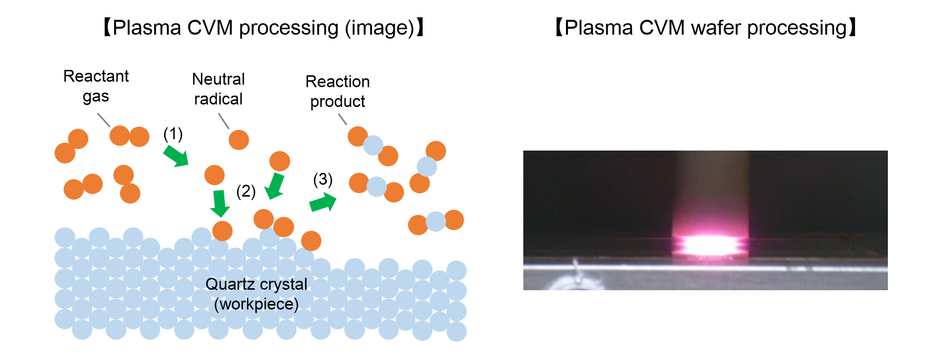
There is a limit to improving the flatness by the lapping process alone. We have introduced plasma CVM processing technology to further improve the processing accuracy. The working principle of this processing is described in (1) to (3) below.
1️⃣ High-density plasma is generated under atmospheric pressure to decompose gas molecules (reactant gas) for processing and generate neutral radicals.
2️⃣ Neutral radicals chemically react with atoms on the surface of a workpiece to generate volatile substances (reaction products).
3️⃣ Reaction products are removed.
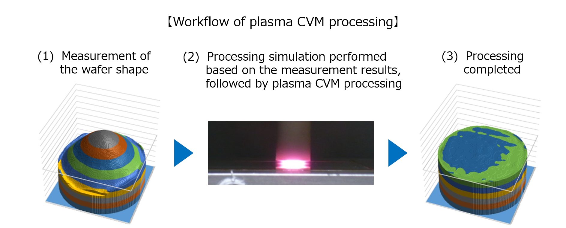
Introduction of plasma CVM processing has further improved the processing accuracy. We have succeeded in reducing the thickness variation by more than 90%. We are confident that this small thickness variation, achieved thanks to our mass production technology, is the best in the industry.