Technology to process synthetic quartz crystals - Realizing the processing of 6-inch wafers -
Increase in the size of quartz crystal wafers
In photolithography, the larger the size of quartz crystal wafers, the larger the number of crystal blanks per wafer, leading to higher productivity.
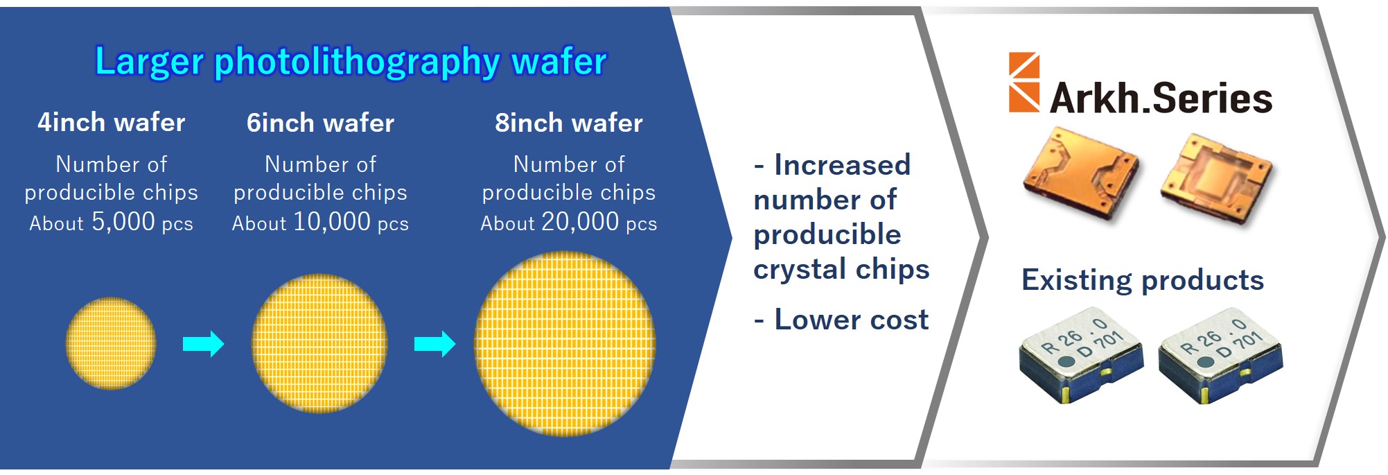
However, the larger the quartz crystal wafers, the more difficult it becomes to process synthetic quartz crystals, such as by cutting and lapping. Such processing cannot be handled by existing equipment. We develop and introduce new equipment to cope with such processing while improving the accuracy of processing technology. However, even if new equipment is introduced, it cannot be used without preparation. Different processing conditions must be established for larger synthetic quartz crystals. It is necessary to conduct various verifications to determine appropriate conditions.
Process to manufacture quartz crystal wafers
The process to manufacture quartz crystal wafers from synthetic quartz crystals is as follows.
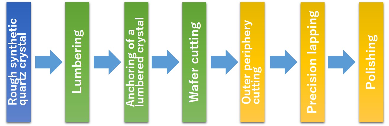
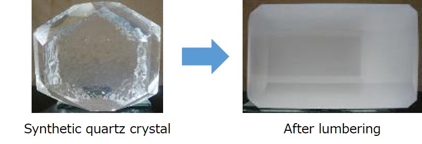
1️⃣ Lumbering
As discussed earlier, quartz crystals have an orientation. The crystal axis must be clarified to ensure functionality as an electronic component. This process is called “lumbering.”
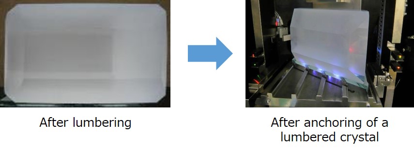
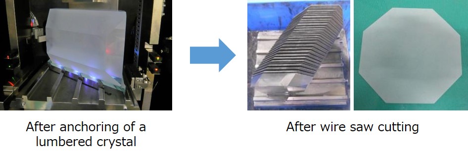
2️⃣ Anchoring of a lumbered crystal
A lumbered synthetic quartz crystal is anchored to the base while measuring and adjusting the angle to achieve cutting at the required angle. The angle measurement accuracy varied due to the increased weight attributed to the larger size of synthetic quartz crystals. To cope with this problem, we improved the accuracy by developing new equipment.
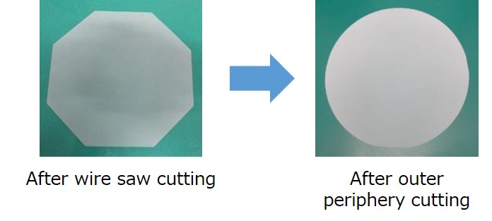
3️⃣ Wafer cutting
Conditions are determined to eliminate waviness and unevenness in the wafers after cutting. A synthetic quartz crystal anchored to the base is cut by a wire saw, which is a device equipped with many wires.
4️⃣ Outer periphery cutting
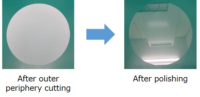
A wafer cut by the wire saw is processed into the shape of a disk.
5️⃣ Precision lapping/polishing
As the finishing process, the quartz crystal wafer disk after outer periphery cutting is subjected to precision lapping/polishing to meet the flatness standard.
Previously, we achieved mass production of 4-inch wafers. However, existing lapping equipment could not cope with 6-inch wafers, which are the largest in the world. We have achieved lapping/polishing of 6-inch wafers by introducing new equipment and optimizing the processing conditions.
Future development
As discussed above, we have developed the capability to grow synthetic quartz crystals for 6-inch wafers, which are the largest in the world, and to polish these wafers. We will promote efforts toward mass production by further improving productivity and processing accuracy and ensure our competitive advantage by increasing the size of quartz crystal wafers as our core technology.