Aiming to Grow the World’s Largest Artificial Crystals
Background to large-sized artificial crystal development
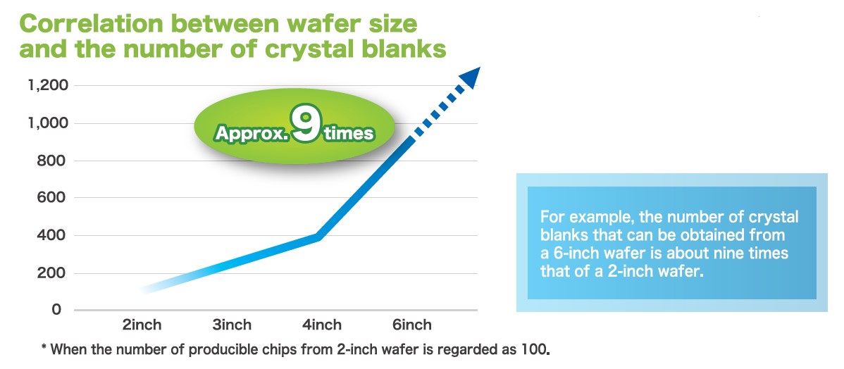
With the advancement of electronics technology, there is an increasing demand for crystal devices that possess small size, high frequency, and high precision.
In the processing of crystal pieces, conventional mechanical methods have encountered difficulties in meeting these requirements. Consequently, there is a growing trend towards the utilization of photolithography, a technique derived from photographic development, which is well-suited for fine processing and widely used in semiconductor manufacturing.
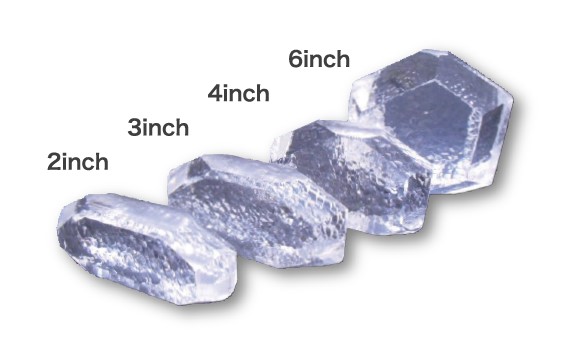
In photolithography, as the wafer size increases, there is an accompanying increase in the yield of crystal pieces per wafer, resulting in improved productivity. Thus, the development of large-sized artificial crystals has become crucial in enhancing a company’s competitiveness.
Issues in large-sized artificial crystal development
Artificial crystals are cultivated by recrystallizing natural crystals onto plate-shaped crystals known as “seed crystals” under high temperature and high pressure conditions. However, merely prolonging the growth time does not guarantee the production of large artificial crystals. The cultivation of large artificial crystals requires seed crystals of an appropriate size to achieve the desired dimensions.
In the past, high-quality sections of natural crystals were processed and used as seed crystals. However, as the desired size increases, acquiring natural crystals suitable for use as seed crystals becomes progressively more challenging. It is not an exaggeration to state that obtaining seed crystals from the natural world for the cultivation of large-sized crystals is nearly impossible.
Challenges and innovations toward solving the problem
In order to address these challenges, we embarked on a journey of “imagination and creativity” to artificially enlarge seed crystals.
We explored the joining of existing seed crystals as a means to achieve this goal. Initially, our efforts in the cultivation process faced continuous failures, such as the occurrence of cracks in the crystals. However, after approximately five years of dedication, we finally succeeded in developing seed crystals that are free from cracks.
However, the development of large-sized artificial crystals was not immediately feasible with these enlarged seed crystals.
Distortions (strains) in the crystal structure emerged at the junctions of the seed crystals, raising concerns about potential impacts on the final product’s properties.
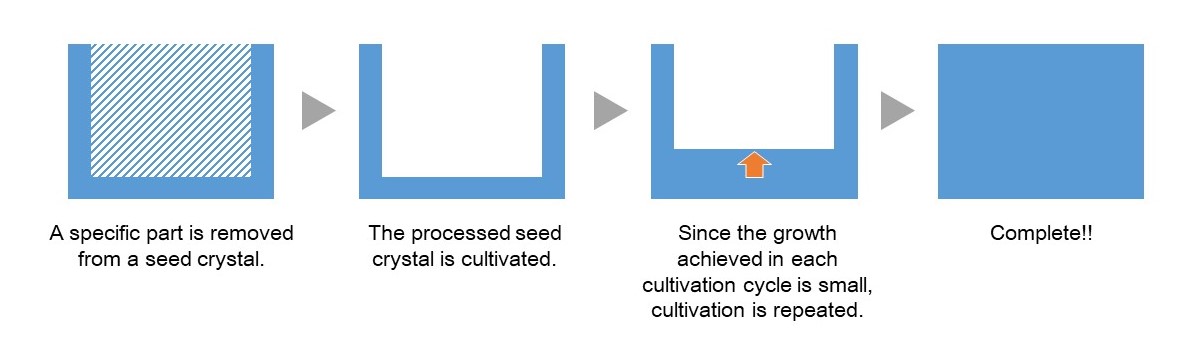
To address this issue, we implemented the frame seed method*1 to enhance the quality of seed crystals, ensuring a crystal structure with minimal distortions and defects.
Crystals possess a property of being more prone or resistant to growth in a specific direction. In the quality improvement process using the frame seed method, it takes a significant amount of time to enlarge seed crystals.
It involved repeated cultivation attempts, and it took approximately five more years from the successful junctions to achieve seed crystals of the desired size. In total, it took over 10 years from the beginning of the project to complete the development of target-sized seed crystals.
*1 Frame seed method
A method of repeating cultivation using a seed crystal from which the central part has been removed in a specific direction
Birth of the world’s largest artificial crystals and advancements toward further enlargement
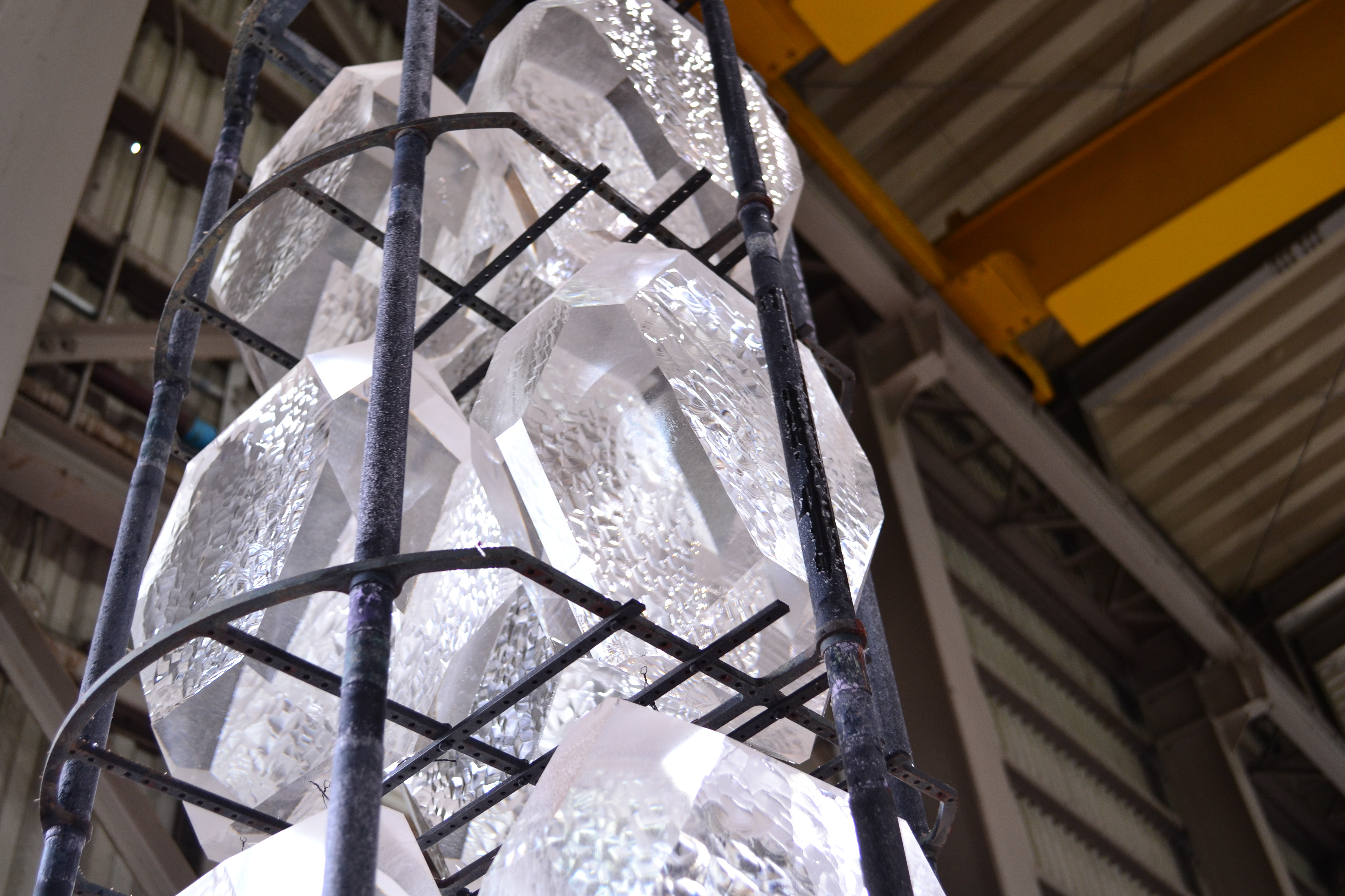
In June 2022, we succeeded in mass-producing the world’s largest artificial crystals for 6-inch wafers using the developed seed crystals, and we are proceeding with their application to our mass-produced products.
Furthermore, we have embarked on the development of even larger artificial crystals for 8-inch wafers.
Although there are significant technological and time barriers to overcome in increasing the sizes of artificial crystals and wafers, we consider this initiative to be of significant importance as it is a core technology for securing our future competitive advantage.
By upsizing crystal wafers, we aim to enhance our cost competitiveness and secure our competitive advantage not only in terms of technology but also in terms of cost.
 |
 |