MO9121


Features
- Any Frequency between 1 to 220 MHz accurate to 6 decimal places
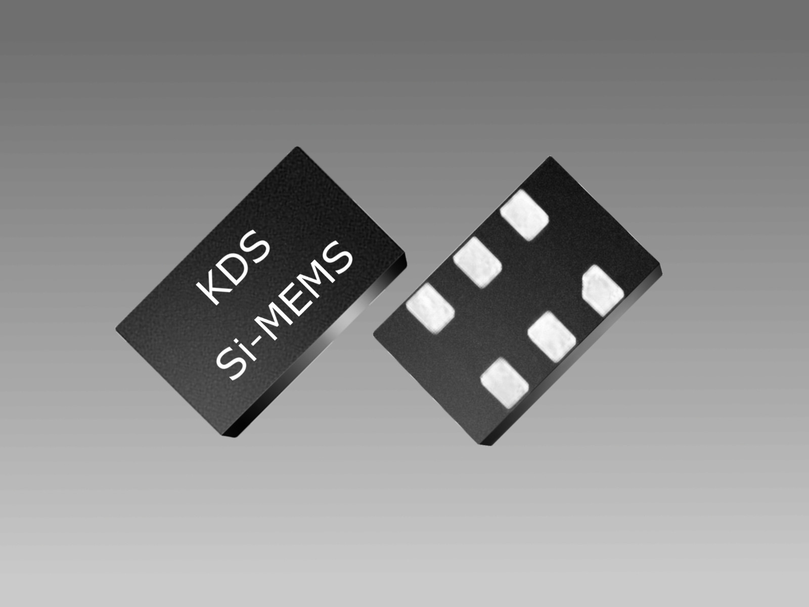
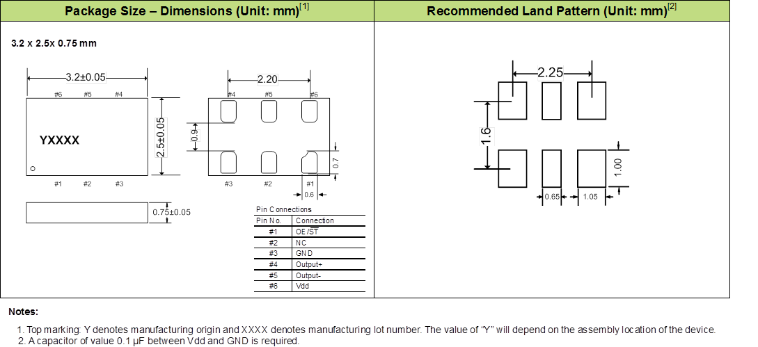
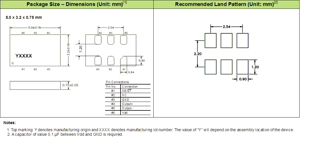
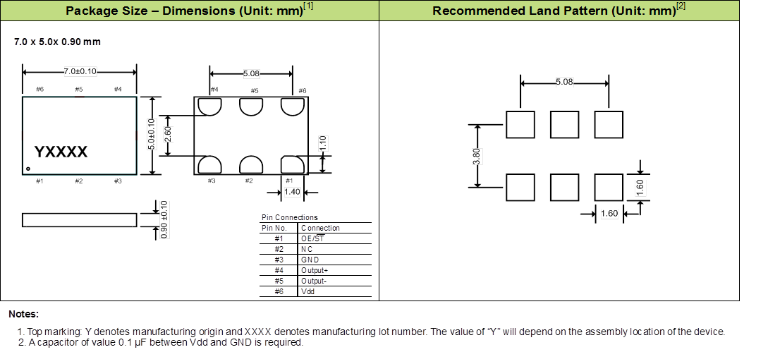
- Industry-Standard packages: 3.2 x 2.5, 5.0 x 3.2 and 7.0 x 5.0 mm
- LVPECL and LVDS output signaling types
- Frequency stability as low as ±10 x 10-6
- 0.6 ps RMS phase jitter (random) over 12 kHz to 20 MHz bandwidth
- For frequencies higher than 220 MHz, refer to MO9122 datasheet
Applications
- Telecom, networking, instrumentation, storage, servers
- 10GB Ethernet, SONET, SATA, SAS, Fibre Channel, PCI-Express
- System Clocking
Standard Specification
| Item | Symbol | Min. | Typ. | Max. | Unit | Condition |
|---|---|---|---|---|---|---|
| Output Frequency Range | f | 25 | - | 212.5 | MHz | Refer to datasheet for exact list of supported frequencies |
| Supply Voltage | Vdd | +2.97 | +3.3 | +3.63 | V | |
| +2.25 | +2.5 | +2.75 | ||||
| +2.25 | - | +3.63 | ||||
| Operating Temperature Range | T_use | -20 | - | +70 | ℃ | Extended Commercial |
| -40 | - | +85 | Industrial | |||
| Frequency Stability | F_stab | -10 | - | +10 | ×10-6 | Inclusive of initial tolerance, operating temperature, rated power supply voltage, and load variations |
| -20 | - | +20 | ||||
| -25 | - | +25 | ||||
| -50 | - | +50 | ||||
| First Year Aging | F_aging1 | -2.0 | - | +2.0 | ×10-6 | TA=+25℃ |
| 10-year Aging | F_aging10 | -5.0 | - | +5.0 | TA=+25℃ | |
| Duty Cycle | DC | 45 | - | 55 | % | |
| Input Low Voltage | VIL | - | - | Vdd × 0.3 | V | Pin 1, OE or ST |
| Input High Voltage | VIH | Vdd × 0.7 | - | - | V | Pin 1, OE or ST |
| Start-up Time | T_start | - | 6.0 | 10 | ms | Measured from the time Vdd reaches its rated minimum value. |
| Resume Time | T_resume | - | 6.0 | 10 | ms | In Standby mode, measured from the time ST pin crosses 50% threshold. |
| LVPECL, DC and AC Characteristics | ||||||
| Current Consumption | Idd | - | +61 | +69 | mA | Excluding Load Termination Current, Vdd = +3.3V or +2.5V |
| OE Disable Supply Current | I_oe | - | - | +35 | mA | OE = Low |
| Standby Current | I_std | - | - | +100 | μA | ST = Low, for all Vdds |
| Output Low Voltage | VOL | Vdd - 1.9 | - | Vdd - 1.5 | V | |
| Output High Voltage | VOH | Vdd - 1.1 | - | Vdd - 0.7 | V | |
| Rise/Fall Time | Tr,Tf | - | 300 | 700 | ps | 20% to 80% |
| OE Enable/Disable Time | T_oe | - | - | 115 | ns | f = 212.5 MHz - For other frequencies, T_oe = 100ns + 3 period |
| RMS Period Jitter | T_jitt | - | 1.2 | 1.7 | ps | f = 100 MHz, Vdd = +3.3V or +2.5V |
| - | 1.2 | 1.7 | f = 156.25 MHz, Vdd = +3.3V or +2.5V | |||
| - | 1.2 | 1.7 | f = 212.5 MHz, Vdd = +3.3V or +2.5V | |||
| RMS Phase Jitter (random) | T_phj | - | 0.6 | 0.85 | ps | f = 156.25 MHz, Integration bandwidth = 12 kHz to 20 MHz, all Vdds |
| LVDS, DC and AC Characteristics | ||||||
| Current Consumption | Idd | - | +47 | +55 | mA | Excluding Load Termination Current, Vdd = +3.3V or +2.5V |
| OE Disable Supply Current | I_oe | - | - | +35 | mA | OE = Low |
| Standby Current | I_std | - | - | +100 | μA | ST = Low, for all Vdds |
| Rise/Fall Time | Tr,Tf | - | 495 | 700 | ps | 20% to 80% |
| Differential Output Voltage | VOD | +250 | +350 | +450 | mV | |
| VOD Magnitude Change | VOD | - | - | +50 | mV | |
| Offset Voltage | VOS | +1.125 | +1.2 | +1.375 | V | |
| VOS Magnitude Change | VOS | - | - | +50 | mV | |
| OE Enable/Disable Time | T_oe | - | - | 115 | ns | f = 212.5 MHz - For other frequencies, T_oe = 100ns + 3 period |
| RMSPeriod Jitter | T_jitt | - | 1.2 | 1.7 | ps | f = 100 MHz, Vdd = +3.3V or +2.5V |
| - | 1.2 | 1.7 | f = 156.25 MHz, Vdd = +3.3V or +2.5V | |||
| - | 1.2 | 1.7 | f = 212.5 MHz, Vdd = +3.3V or +2.5V | |||
| RMS Phase Jitter (random) | T_phj | - | 0.6 | 0.85 | ps | f = 156.25 MHz, Integration bandwidth = 12 kHz to 20 MHz, all Vdds |
| Packing Unit | 1000pcs./reel(φ180)or 3000pcs./reel(φ180 : 3225 package) | |||||
Consult our sales representative for other specifications.
Dimentions, etc. (Click for full size)
Reference
TEL:+81-79-425-3141
FAX:+81-79-425-1134
FAX:+81-79-425-1134