MO8021


Features
- 1 to 26 MHz with 6 decimal places of accuracy
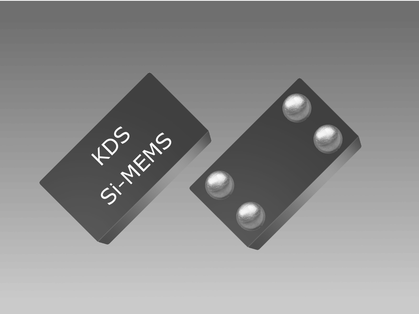
- Ultra-small 1.5 mm x 0.8 mm package
- Ultra-low current consumption of +60 μA at 3.072 MHz
- Operating temperature from -40°C to +85°C
- Frequency stability as low as ±100 x 10-6
Applications
- Tablets, Wearables, Fitness band, Portable audio
- Health and medical monitoring
- IoT devices
- Input devices
Standard Specification
| Item | symbol | Min. | Typ. | Max. | Unit | Condition |
|---|---|---|---|---|---|---|
| Output Frequency Range | f | 1 | - | 26 | MHz | |
| Supply Voltage | Vdd | +1.62 | +1.8 | +1.98 | V | |
| Operating Temperature Range |
T_use | -20 | - | +70 | ℃ | Extended Commercial |
| -40 | - | +85 | Industrial | |||
| Frequency Tolerance | F_tol | -15 | - | +15 | ×10-6 | Frequency offset at +25°C post reflow |
| Frequency Stability | F_stab | -100 | - | +100 | ×10-6 | Inclusive of initial tolerance, and variations over operating temperature, rated power supply voltage and output load. |
| First Year Aging | f_1year | -3.0 | - | +3.0 | ×10-6 | TA = +25°C |
| Current Consumption[1] | Idd | - | +60 | - | μA | f = 3.072 MHz, no load |
| - | +110 | +130 | f = 6.144 MHz, no load | |||
| - | +230 | +270 | f = 6.144 MHz, 10 pF load | |||
| - | - | +160 | f = 6.144 MHz, Vdd = +2.25 to +3.63V, no load | |||
| - | +160 | - | f = 12 MHz, no load | |||
| Standby Current | I_std | - | +0.7 | +1.3 | μA | Vdd = +1.8V, ST pin = HIGH, output is weakly pulled down |
| - | - | +1.5 | Vdd = +2.25 to +3.63V, ST pin = HIGH, output is weakly pulled down | |||
| Duty Cycle | DC | 45 | - | 55 | % | |
| Output Low Voltage | VOL | - | - | Vdd x 0.1 | V | IOL = +0.5 mA (Vdd = +1.8V) IOL = +1.2 mA (Vdd = +2.25 to +3.63V) |
| Output High Voltage | VOH | Vdd x 0.9 | - | - | V | IOH = -0.5 mA (Vdd = +1.8V) IOH = -1.2 mA (Vdd = +2.25 to +3.63V) |
| Rise/Fall Time | Tr,Tf | - | +4.0 | +8.0 | ns | Vdd = +1.8V, 20% - 80%. Contact KDS for other programmable rise/fall options |
| - | - | +8.0 | Vdd = +2.25 to +3.63V, 20% - 80%. Contact KDS for other programmable rise/fall options | |||
| Input Low Voltage | VIL | - | - | Vdd x 0.2 | V | |
| Input High Voltage | VIH | Vdd × 0.8 | - | - | V | |
| Startup Time | T_start | - | 75 | 150 | ms | Measured from the time Vdd reaches 90% of its final value |
| Standby Time | T_stdby | - | - | 20 | μs | Measured from the time ST pin crosses 50% threshold |
| Resume Time | T_resume | - | 2.0 | 3.0 | ms | Measured from the time ST pin crosses 50% threshold |
| RMS Period Jitter | T_jitt | - | 75 | 110 | ps | f = 6.144 MHz, Vdd = +1.8V |
| - | - | 110 | f = 6.144 MHz, Vdd = +2.25 to +3.63V | |||
| RMS Phase Jitter (random) | T_phj | - | 0.8 | 2.5 | ns | f = 6.144 MHz, Vdd = +1.8V Integration bandwidth = 100 Hz to 40 kHz[2] |
| - | - | 2.5 | f = 6.144 MHz, Vdd = +2.25 to +3.63V Integration bandwidth = 100 Hz to 40 kHz[2] |
|||
| Packing Unit | 1000pcs./reel(φ180)or 3000pcs./reel(φ180) | |||||
[1]. Current consumption with load is a function of the output frequency and output load.
For any given output frequency, the capacitive loading will increase current consumption equal toC_load*Vdd*f(MHz).
[2]. Max spec inclusive of +25 mV peak-to-peak sinusoidal noise on Vdd. Noise frequency 100 Hz to 20 MHz.
Consult our sales representative for other specifications.
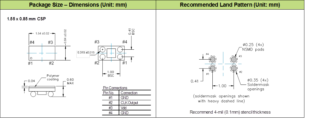
Dimentions, etc. (Click for full size)
Reference
TEL:+81-79-425-3141
FAX:+81-79-425-1134
FAX:+81-79-425-1134