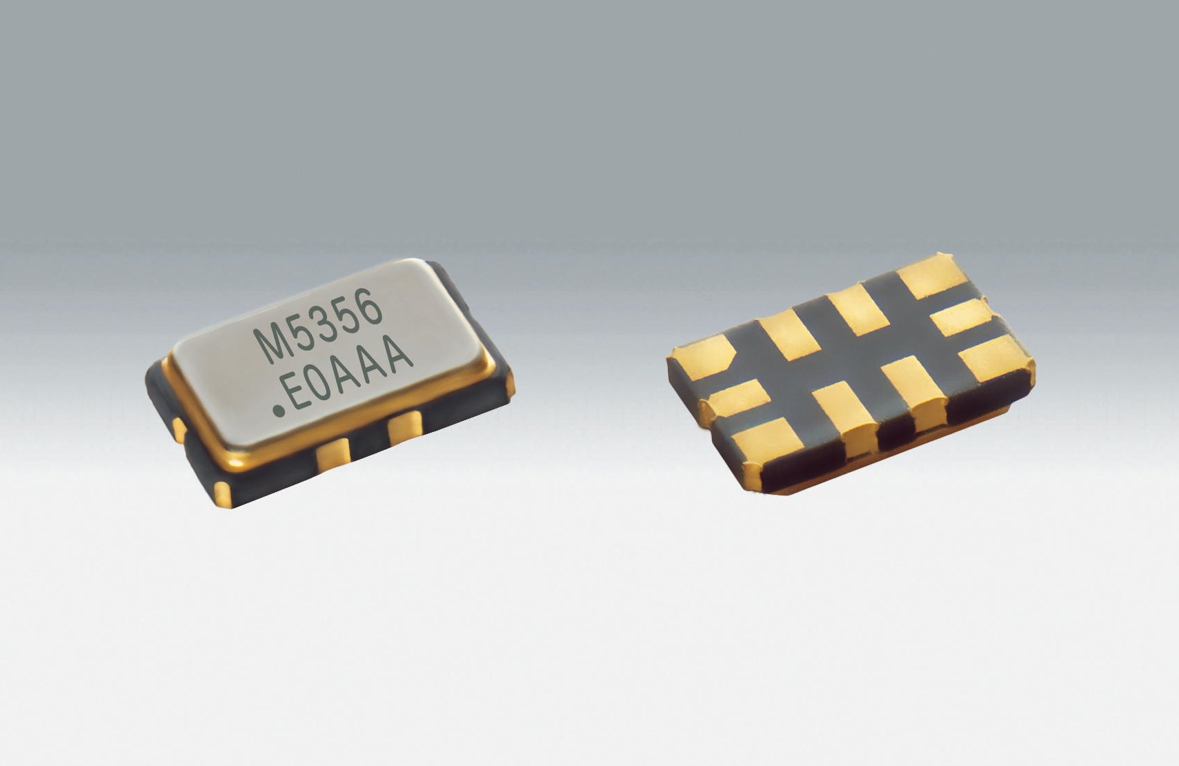
MO5359


Features
- Output 60 to 189 MHz, and 200 to 220 MHz, in 1Hz steps
- ±50 x 10-9 over-temperature stability
- ±1.0x10⁻⁹/℃ frequency slope (ΔF/ΔT)
- 0℃ to +70℃ operating temperature
- LVCMOS or Clipped Sinewave output
Applications
- 4G/5G radio, Small cell
- IEEE1588 boundary and grandmaster clocks
- Carrier-grade routers and switches
- Synchronous Ethernet
- Optical transport-SONET/SDH, OTN, Stratum3
- DOCSIS 3.x remote PHY
- GPS disciplined oscillators, Precision GNSS systems
Standard Specification
| Item | Symbol | Min. | Typ. | Max. | Unit | Condition |
|---|---|---|---|---|---|---|
| Output Frequency Range | f | 60.000001 | - | 189 | MHz | |
| 200 | - | 220 | ||||
| Supply Voltage | Vdd | +2.97 | +3.3 | +3.63 | V | Contact KDS for +2.25V to +3.63V continuous supply voltage support |
| +2.7 | +3.0 | +3.3 | ||||
| +2.52 | +2.8 | +3.08 | ||||
| +2.25 | +2.5 | +2.75 | ||||
| Operating Temperature Range | T_use | 0 | - | +70 | ℃ | Commercial, ambient temperature |
| Initial Tolerance | F_int | -0.5 | - | +0.5 | ×10-6 | Initial frequency at +25℃ inclusive of solder-down shift at 48 hours after 2 reflows |
| Frequency Stability over temperature | F_stab | -50 | - | +50 | ×10-9 | Referenced to (fmax + fmin)/2 over the specified temperature range |
| Frist Year Aging | F_aging1 | - | ±0.3 | - | ×10-6 | TA = +25℃ |
| Pull range | PR | ±6.25 | ×10-6 | VC TC-MO mode. Contact KDS for ±12.5, ±25 x 10-6 | ||
| ±6.25, ±10, ±12.5,±25, ±50, ±80, ±100, ±125, ±150, ±200, ±400, ±600, ±800, ±1200, ±1600, ±3200 | DCTC-MO mode. | |||||
| Lower control voltage | VC_L | - | - | Vdd x 0.1 | V | |
| Upper control voltage | VC_U | Vdd x 0.9 | - | - | V | |
| Control voltage input impedance | VC_z | 8 | - | - | MΩ | |
| Control voltage input bandwidth | VC_c | - | 10 | - | kHz | |
| Frequency Change Polarity | - | Positive Slope | - | |||
| Current Consumption | Idd | - | +48 | +62 | mA | F = 100MHz, No Load, TC-MO and DC TC-MO mode. |
| - | +52 | +66 | F = 100MHz, No Load, VC TC-MO mode. | |||
| OE Disable Current | I_od | - | +45 | +52 | mA | OE = GND, output is weakly pull down,TC-MO and DC TC-MO mode. |
| - | +49 | +56 | OE = GND, output is weakly pull down, VC TC-MO mode. | |||
| Input Low voltage | VIL | - | - | Vdd x 0.3 | V | |
| Input High voltage | VIH | Vdd x 0.7 | - | - | V | |
| Start-up Time | T_start | - | 2.5 | 3.5 | ms | Time to first pulse, measured from the time Vdd reaches 90% of its final value |
| Duty Cycle | DC | 45 | - | 55 | % | |
| Output Low Voltage | VOL | - | - | Vdd x 0.1 | V | IOL = -3mA |
| Output High Voltage | VOH | Vdd x 0.9 | - | - | V | IOH = +3mA |
| Rise and Fall Time | Tr,Tf | 0.8 | 1.2 | 1.9 | ps | 10% to 90% Vdd |
| RMS Period Jitter | T_jitt | - | 1.0 | 1.8 | ps | f = 100MHz per JESD65 standard |
| RMS Phase Jitter (Random) | T_phj | - | 0.31 | 0.48 | ps | f = 100MHz, Integration bandwidth = 12kHz to 20MHz, -40 to +85℃ |
| Packing Unit | 1000pcs./reel (φ180) | |||||
Consult our sales representative for other specifications.
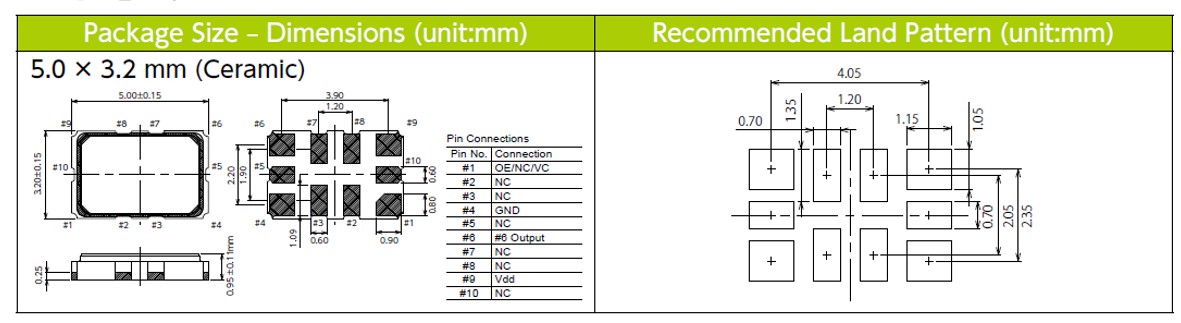
外形尺寸等 (点击看大图)
参考
TEL:+81-79-425-3141
FAX:+81-79-425-1134
FAX:+81-79-425-1134