MO3808


Features
- Any frequency between 1MHz and 80MHz with 6 decimal places of accuracy
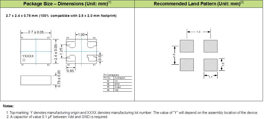
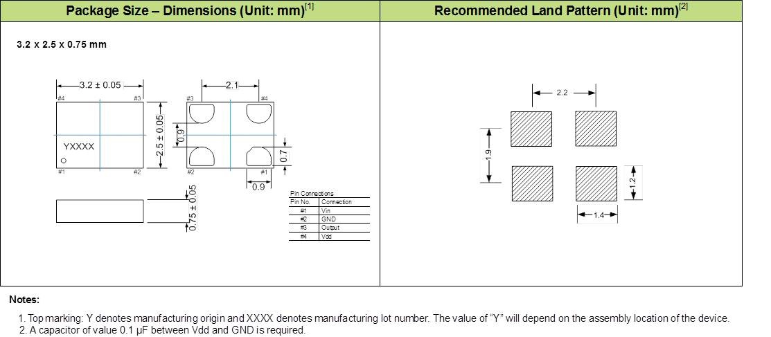
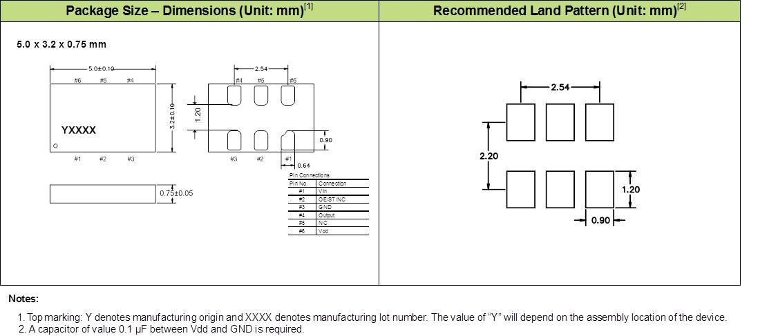
- Four industry-standard packages:
2.7 x 2.4 mm (4-pin, compatible with 2.5 x 2.0 mm footprint)
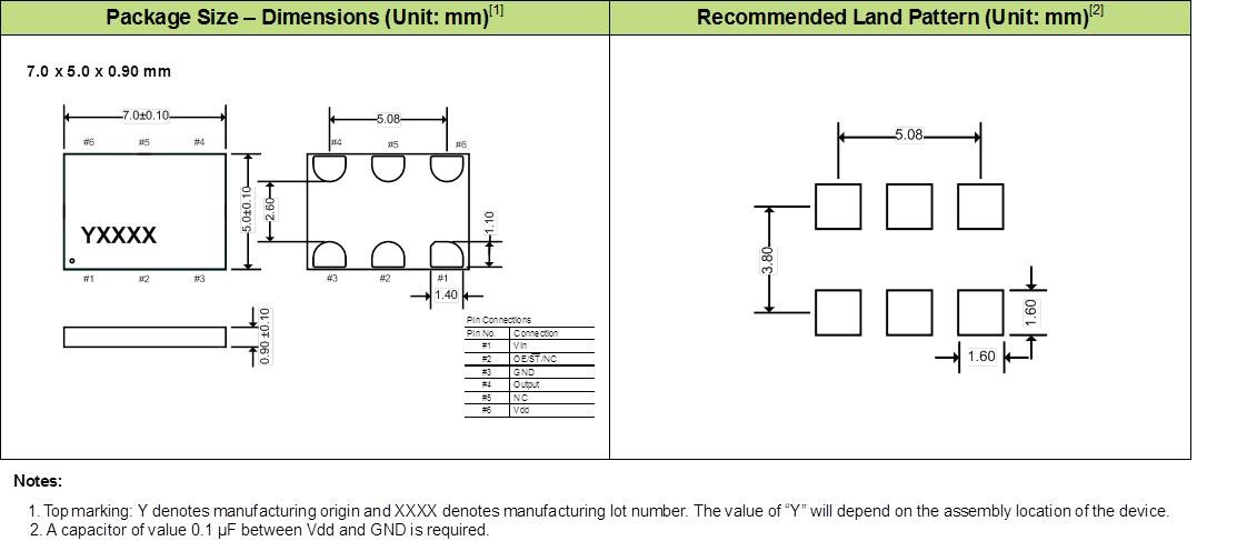
3.2 x 2.5 mm (4-pin), 5.0 x 3.2 mm (6-pin), 7.0 x 5.0 mm (6-pin) - Frequency stability as tight as ±10 x 10-6
- Widest pull range options from ±25 to ±1600 x 10-6
Applications
- Telecom clock synchronization, instrumentation
- Low bandwidth analog PLL, jitter cleaner, clock recovery, audio
- Video, 3G/HD-SDI, FPGA, broadband and networking
Standard Specification[1,2,3]
| Item | Symbol | Min. | Typ. | Max. | Unit | Condition |
|---|---|---|---|---|---|---|
| Output Frequency Range | f | 1 | - | 80 | MHz | |
| Supply Voltage | Vdd | +1.71 | +1.8 | +1.89 | V | Additional supply voltages between +2.5V and +3.3V can be supported. |
| +2.25 | +2.5 | +2.75 | ||||
| +2.52 | +2.8 | +3.08 | ||||
| +2.97 | +3.3 | +3.63 | ||||
| Operating Temperature Range | T_use | -20 | - | +70 | ℃ | Extended Commercial |
| -40 | - | +85 | Industrial | |||
| Frequency Stability | F_stab | -10 | - | +10 | ×10-6 | Inclusive of Initial tolerance[4] at +25°C, and variation over temperature, rated supply voltage and load. |
| -25 | - | +25 | ||||
| -50 | - | +50 | ||||
| 10-year Aging | F_aging10 | -5.0 | - | +5.0 | ×10-6 | 10 years, TA = +25°C |
| Current Consumption | Idd | - | +31 | +33 | mA | No load condition, f = 20 MHz, Vdd = +2.5V, +2.8V or +3.3V |
| - | +29 | +31 | No load condition, f = 20 MHz, Vdd = +1.8V | |||
| Standby Current | I_std | - | - | +70 | μA | Vdd = +2.5V, +2.8V or +3.3V, ST = GND, Output is weakly pulled down |
| - | - | +10 | Vdd = +1.8V, ST = GND, Output is weakly pulled down | |||
| Duty Cycle | DC | 45 | - | 55 | % | All Vdds |
| Output Low Voltage | VOL | - | - | Vdd x 0.1 | V | IOL = +7.0 mA (Vdd = +3.0V or +3.3V) IOL = +4.0 mA (Vdd = +2.8V or +2.5V) IOL = +2.0 mA (Vdd = +1.8V) |
| Output High Voltage | VOH | Vdd x 0.9 | - | - | V | IOH = -7.0 mA (Vdd = +3.0V or +3.3V) IOH = -4.0 mA (Vdd = +2.8V or +2.5V) IOH = -2.0 mA (Vdd = +1.8V) |
| Rise/Fall Time | Tr,Tf | - | 1.5 | 2.0 | ns | Vdd = +1.8V, +2.5v, +2.8V or +3.3V, 10% - 90% Vdd level |
| Pull Range[5,6] | PR | ±25, ±50, ±100, ±150, ±200,±400,±800,±1600 | ×10-6 | See the Absolute Pull Range and APR table of datasheet | ||
| Upper Control Voltage | VC_U | +1.7 | - | - | V | Vdd = +1.8V, Voltage at which maximum deviation is guaranteed. |
| +2.4 | - | - | Vdd = +2.5V, Voltage at which maximum deviation is guaranteed. | |||
| +2.7 | - | - | Vdd = +2.8V, Voltage at which maximum deviation is guaranteed. | |||
| +3.2 | - | - | Vdd = +3.3V, Voltage at which maximum deviation is guaranteed. | |||
| Lower Control Voltage | VC_L | - | - | +0.1 | V | Voltage at which minimum deviation is guaranteed. |
| Control Voltage Input Impedance | Z_in | 100 | - | - | kΩ | |
| Control Voltage Input Capacitance | C_in | - | 5.0 | 3.0 | pF | |
| Linearity | Lin | - | 0.1 | 1.0 | % | |
| Frequency Change Polarity | - | Positive slope | - | |||
| Startup Time | T_start | - | - | 10 | ms | |
| OE Enable/Disable Time | T_oe | - | - | 180 | ns | f = 40MHz, all Vdds, For other freq., T_oe = 100 ns + 3 clock periods |
| Resume Time | T_resume | - | 7.0 | 10 | ms | |
| RMS Period Jitter | T_jitt | - | 1.5 | 2.0 | ps | f = 20MHz, Vdd = +2.5V, +2.8V or +3.3V |
| - | 2.0 | 3.0 | f = 20MHz, Vdd = +1.8V | |||
| RMS Phase Jitter (random) | T_phj | - | 0.5 | 1.0 | ps | f = 20MHz, Integration bandwidth = 12kHz to 20MHz, All Vdds |
| Packing Unit | 1000pcs./reel(φ180)or 3000pcs./reel(φ180 : 2724, 3225 package) | |||||
[1]. All electrical specifications in the above table are specified with 15 pF output load and for all Vdd(s) unless otherwise stated.
[2]. The typical value of any parameter in the Electrical Characteristics table is specified for the nominal value of the highest voltage option for that parameter and at +25 °C temperature.
[3]. All max and min specifications are guaranteed across rated voltage variations and operating temperature ranges, unless specified otherwise
[4]. Initial tolerance is measured at Vin = Vdd/2
[5]. Absolute Pull Range (APR) is defined as the guaranteed pull range over temperature and voltage.
[6]. APR = pull range (PR) - frequency stability (F_stab) - Aging (F_aging)
Consult our sales representative for other specifications.
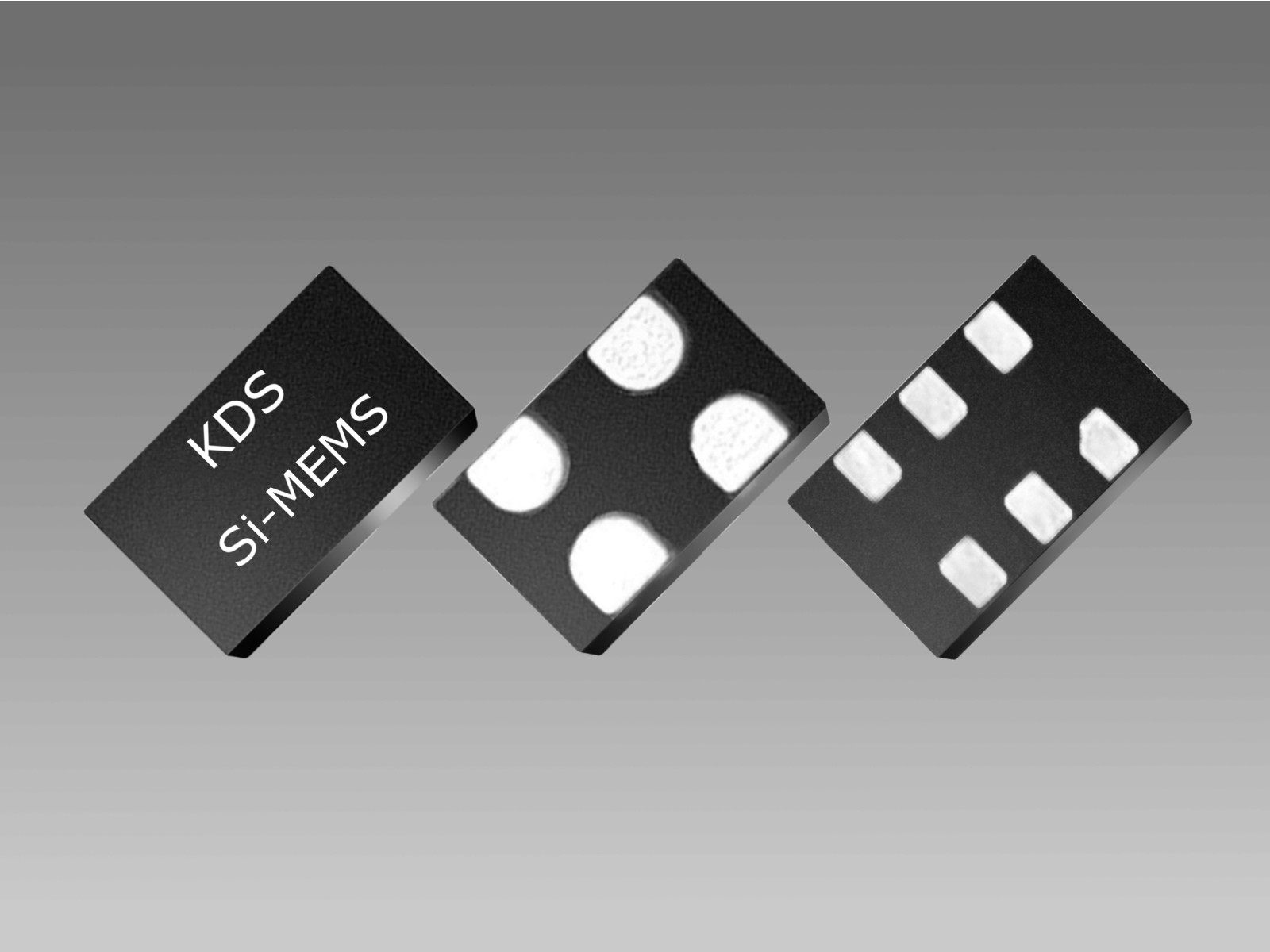
Dimentions, etc. (Click for full size)
Reference
FAX:+81-79-425-1134