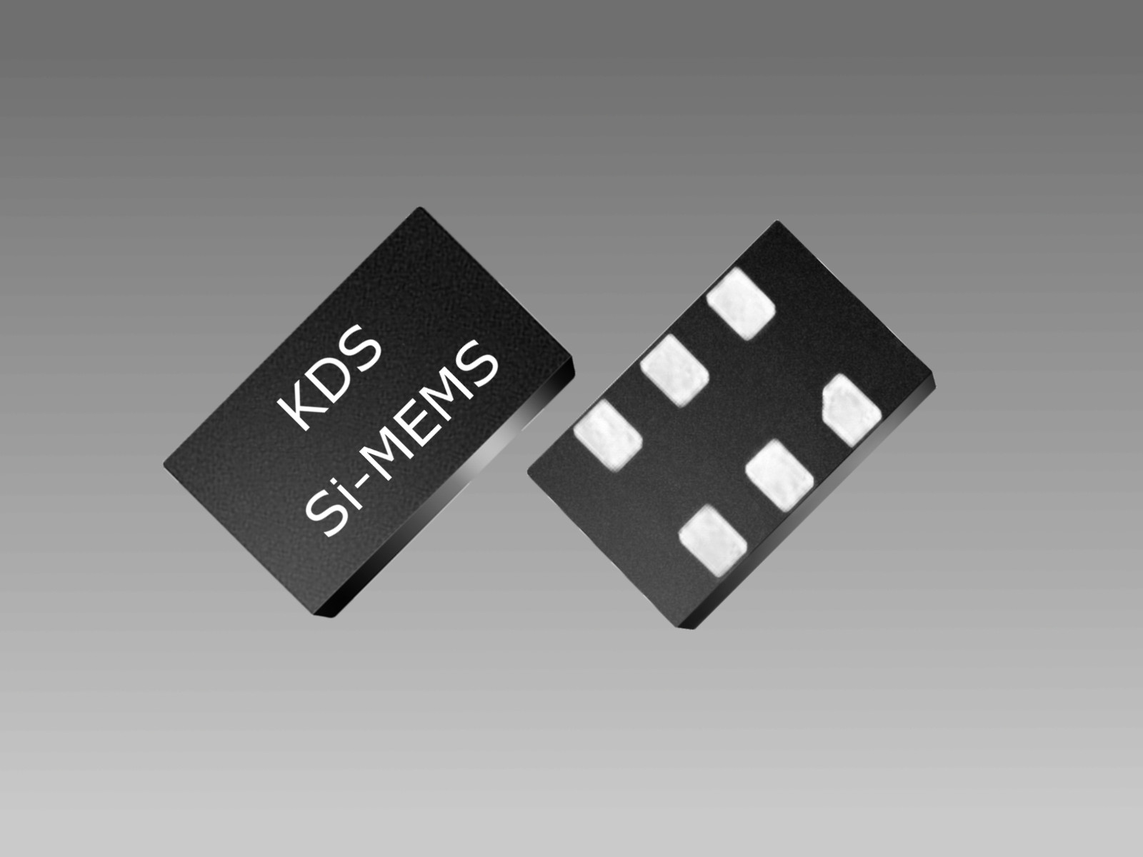
MO3373


Features
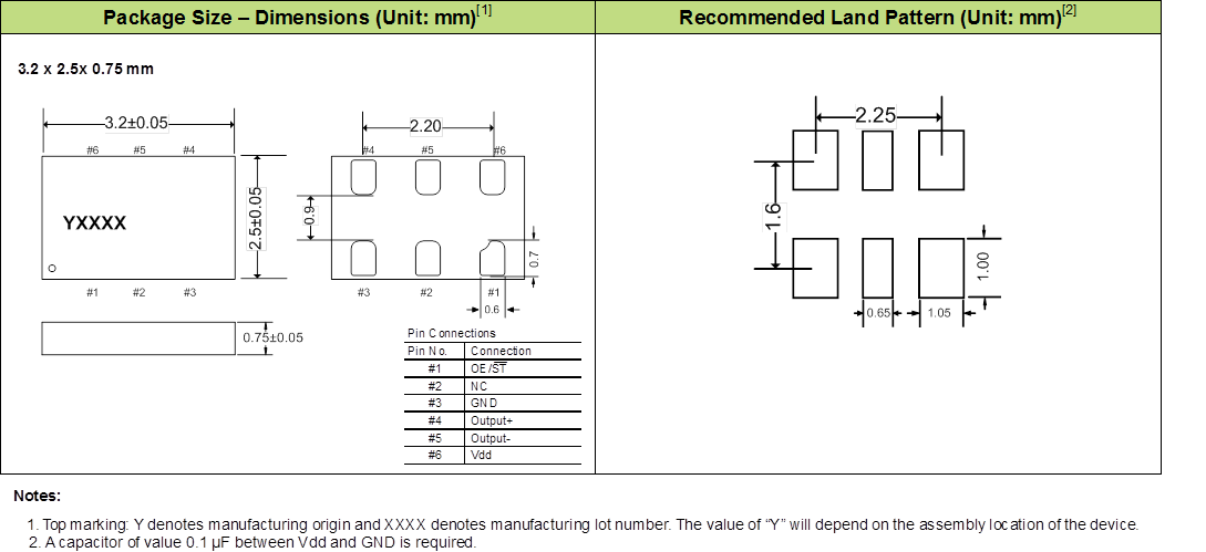
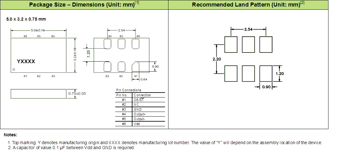
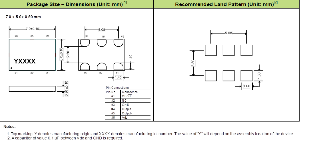
- Industry-Standard packages: 3.2 x 2.5 mm, 5.0 x 3.2 mm, 7.0 x 5.0 mm
- Widest pull range options: ±25, ±50, ±80, ±100, ±150, ±200, ±400, ±800, ±1600, ±3200 x 10-6
- 0.23 ps RMS phase jitter (Typ.)
Applications
- Telecom clock synchronization, instrumentation
- Low bandwidth analog PLL, jitter cleaner, clock recovery, audio
- Video, 3G/HD-SDI, FPGA, broadband and networking
Standard Specification
| Item | Symbol | Min. | Typ. | Max. | Unit | Condition |
|---|---|---|---|---|---|---|
| Output Frequency Range | f | 220 | - | 725 | MHz | Accurate to 6 decimal places |
| Supply Voltage | Vdd | +2.97 | +3.3 | +3.63 | V | |
| +2.7 | +3.0 | +3.3 | ||||
| +2.52 | +2.8 | +3.08 | ||||
| +2.25 | +2.5 | +2.75 | ||||
| Operating Temperature Range | T_use | -20 | - | +70 | ℃ | Extended Commercial |
| -40 | - | +85 | Industrial | |||
| -40 | - | +95 | ||||
| -40 | - | +105 | Extended Industrial | |||
| Frequency Stability | F_stab | -15 | - | +15 | ×10-6 | Inclusive of initial tolerance, operating temperature, rated power supply voltage, load variations, and first year aging at +25°C condition |
| -25 | - | +25 | ||||
| -35 | - | +35 | ||||
| -50 | - | +50 | ||||
| Duty Cycle | DC | 45 | - | 55 | % | |
| Input Low Voltage | VIL | - | - | Vdd x 0.3 | V | Pin 2, OE |
| Input High Voltage | VIH | Vdd × 0.7 | - | - | V | Pin 2, OE |
| Start-up Time | T_start | - | - | 3.0 | ms | Measured from the time Vdd reaches its rated minimum value. |
| Enable and Disable Time | T_oe | - | - | 3.8 | μs | f = 322.265625 MHz |
| Pull Range | PR | ±25, ±50, ±80, ±100, ±150, ±200, ±400, ±800, ±1600, ±3200 |
×10-6 | |||
| Output Disable Leakage Current | I_leak | - | +0.15 | - | μA | OE = Low |
| Lower Control Voltage | VC_L | - | - | Vdd x 0.1 | V | Voltage at which minimum frequency deviation is guaranteed |
| Upper Control Voltage | VC_U | Vdd x 0.9 | - | - | V | Voltage at which maximum frequency deviation is guaranteed |
| Control Voltage Input Impedance | VC_z | - | 10 | - | MΩ | |
| Control Voltage Input Bandwidth | V_c | - | 10 | - | kHz | |
| Pull Range Linearity | Lin | - | - | 1 | % | |
| Frequency Change Polarity | - | Positive Slope | - | |||
| LVPECL Specific | ||||||
| Current Consumption | Idd | - | - | +97 | mA | Excluding Load Termination Current, Vdd = +3.3V or +2.5V |
| OE Disable Supply Current | I_oe | - | - | +63 | mA | OE = Low |
| Maximum Output Current | I_driver | - | - | +32 | mA | Maximum average current drawn from OUT+ or OUT- |
| OUTOutput Low Voltage |
VOL | Vdd - 1.9 | - | Vdd - 1.5 | V | |
| Output High Voltage | VOH | Vdd - 1.15 | - | Vdd - 0.7 | V | |
| Output Differential Voltage Swing | V_Swing | +1.2 | +1.6 | +2.0 | V | |
| Rise and Fall Time | Tr,Tf | - | 225 | 290 | ps | 20% to 80% |
| RMS Period Jitter [1] | T_jitt | - | 1.0 | 1.6 | ps | f = 322.265625 MHz, Vdd = +3.3V or +2.5V |
| RMS Phase Jitter (random) | T_phj | - | 0.225 | 0.282 | ps | Note [2] |
| LVDS Specific | ||||||
| Current Consumption | Idd | - | - | +89 | mA | Excluding Load Termination Current, Vdd = +3.3V or +2.5V |
| OE Disable Supply Current | I_oe | - | - | +67 | mA | OE = Low |
| Rise and Fall Time | Tr,Tf | - | 370 | 470 | ps | Measured with 2pF capacitive loading to GND, 20% to 80% |
| Differential Output Voltage | VOD | +250 | - | +450 | mV | |
| VOD Magnitude Change | ⊿VOD | - | - | +50 | mV | |
| Offset Voltage | VOS | +1.125 | - | +1.375 | V | |
| VOS Magnitude Change | ⊿VOS | - | - | +50 | mV | |
| RMS Period Jitter [1] | T_jitt | - | 0.92 | 1.6 | ps | f = 322.265625 MHz, Vdd = +3.3V or +2.5V |
| RMS Phase Jitter (random) | T_phj | - | 0.235 | 0.282 | ps | Note [2] |
| HCSL Specific | ||||||
| Current Consumption | Idd | - | - | +102 | mA | Excluding Load Termination Current, Vdd = +3.3V or +2.5V |
| OE Disable Supply Current | I_oe | - | - | +67 | mA | OE = Low |
| Rise and Fall Time | Tr,Tf | - | 360 | 470 | ps | Measured with 2pF capacitive loading to GND, 20% to 80% |
| Output Low Voltage | VOL | -0.05 | - | +0.08 | V | |
| Output High Voltage | VOH | +0.6 | - | +0.9 | V | |
| Output Differential Voltage Swing | V_Swing | +1.2 | +1.4 | +1.8 | V | |
| RMS Period Jitter [1] | T_jitt | - | 1.0 | 1.6 | ps | f = 322.265625 MHz, Vdd = +3.3V or +2.5V |
| RMS Phase Jitter (random) | T_phj | - | 0.235 | 0.282 | ps | Note [2] |
| Packing Unit | 1000pcs./reel (φ180) or 3000pcs./reel (φ180: 3225 package) | |||||
[1]. Measured according to JESD65B
[2]. 5.0×3.2 and 3.2×2.5 mm package, f = 322.265625 MHz, Integration bandwidth = 12 kHz to 20 MHz, all Vdd levels, includes spurs. Temperature ranges -20 to +70ºC and -40 to +85℃
Consult our sales representative for other specifications.
Dimentions, etc. (Click for full size)
Reference
TEL:+81-79-425-3141
FAX:+81-79-425-1134
FAX:+81-79-425-1134