MO2002


优点
- Any Frequency between 115 to 137 MHz accurate to 6 decimal places
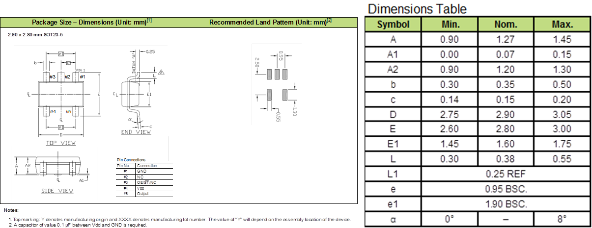
- 5-pin SOT23-5 : 2.9 mm x 2.8 mm
- Excellent total frequency stability as low as ±20 x 10-6
- Low power consumption of +4.9 mA typical at f = 125 MHz, Vdd = +1.8V
用途
- Industrial and Medical devices
- SSD , Routers, Storage servers
- GPON,EPON, SATA/SAS, Ethernet
- PCI, PCI-E, DDR
一般规格
| Item | Symbol | Min. | Typ. | Max. | Unit | Condition |
|---|---|---|---|---|---|---|
| Output Frequency Range | f | 115 | - | 137 | MHz | |
| Supply Voltage | Vdd | +1.62 | +1.8 | +1.98 | V | |
| +2.25 | +2.5 | +2.75 | ||||
| +2.52 | +2.8 | +3.08 | ||||
| +2.7 | +3.0 | +3.3 | ||||
| +2.97 | +3.3 | +3.63 | ||||
| +2.25 | - | +3.63 | ||||
| Frequency Stability | F_stab | -20 | - | +20 | ×10-6 | Inclusive of Initial tolerance at +25°C, 1st year aging at +25°C, and variations over operating temperature, rated power supply voltage and load (15 pF ± 10%). |
| -25 | - | +25 | ||||
| -50 | - | +50 | ||||
| Current Consumption | Idd | - | +6.2 | +7.5 | mA | No load condition, f = 125 MHz, Vdd =+2.8V, +3.0V or +2.25V to +3.36V |
| - | +5.5 | +6.4 | No load condition, f = 125 MHz, Vdd = +2.5V | |||
| - | +4.9 | +5.6 | No load condition, f = 125 MHz, Vdd = +1.8V | |||
| OE Disable Current | I_od | - | - | +4.3 | mA | Vdd = +2.5V to +3.3V, OE = Low, Output in high Z state |
| - | - | +4.1 | Vdd = +1.8V, OE = Low, Output in high Z state | |||
| Standby Current | I_std | - | +2.6 | +4.3 | μA | Vdd = +2.8V to +3.3V, ST = Low, Output is weakly pulled down |
| - | +1.4 | +2.5 | Vdd = +2.5V, ST = Low, Output is weakly pulled down | |||
| - | +0.6 | +1.3 | Vdd = +1.8V, ST = Low, Output is weakly pulled down | |||
| Duty Cycle | DC | 45 | - | 55 | % | All Vdds |
| Output Low Voltage | VOL | - | - | Vdd x 0.1 | V | IOL= +4.0 mA (Vdd = +3.0V or +3.3V) IOL = +3.0 mA (Vdd = +2.8V or +2.5V) IOL = +2.0 mA (Vdd = +1.8V) |
| Output High Voltage | VOH | Vdd x 0.9 | - | - | V | IOH = -4.0 mA (Vdd = +3.0V or +3.3V) IOH = -3.0 mA (Vdd = +2.8V or +2.5V) IOH = -2.0 mA (Vdd = +1.8V) |
| Rise/Fall Time | Tr,Tf | - | 1.0 | 2.0 | ns | Vdd = +2.5V, +2.8V, +3.0V or +3.3V, 20% - 80% |
| - | 1.3 | 2.5 | Vdd =+1.8V, 20% - 80% | |||
| - | 1.0 | 3.0 | Vdd = +2.25V - +3.63V, 20% - 80% | |||
| Input Low Voltage | VIL | - | - | Vdd x 0.3 | V | Pin 3, OE or ST |
| Input High Voltage | VIH | Vdd × 0.7 | - | - | V | Pin 3, OE or ST |
| Startup Time | T_start | - | - | 5.0 | ms | Measured from the time Vdd reaches its rated minimum value |
| Enable/Disable Time | T_oe | - | - | 130 | ns | f = 115 MHz. For other frequencies, T_oe = 100 ns + 3 * clock periods |
| Resume Time | T_resume | - | - | 5.0 | ms | Measured from the time ST pin crosses 50% threshold |
| RMS Period Jitter | T_jitt | - | 1.9 | 3.0 | ps | f = 125 MHz, Vdd = +2.5V, +2.8V, +3.0V or +3.3V |
| - | 1.6 | 4.0 | f = 125 MHz, Vdd = +1.8V | |||
| Peak-to-peak Period Jitter | T_pk | - | 12 | 20 | ps | f = 125 MHz, Vdd = +2.5V, +2.8V, +3.0V or +3.3V |
| - | 14 | 30 | f = 125 MHz, Vdd = +1.8V | |||
| RMS Phase Jitter (random) | T_phj | - | 0.5 | 0.9 | ps | Integration bandwidth = 900 kHz to 7.5 MHz |
| - | 1.3 | 2.0 | Integration bandwidth = 12 kHz to 20 MHz | |||
| Packing Unit | 1000pcs./reel(φ180)or 3000pcs./reel(φ180) | |||||
Consult our sales representative for other specifications.
外形尺寸等 (点击看大图)
参考
TEL:+81-79-425-3141
FAX:+81-79-425-1134
FAX:+81-79-425-1134