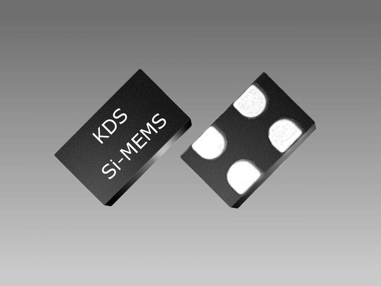
MO1602


Features
- 52 standard frequencies between 3.57 MHz and 77.76 MHz
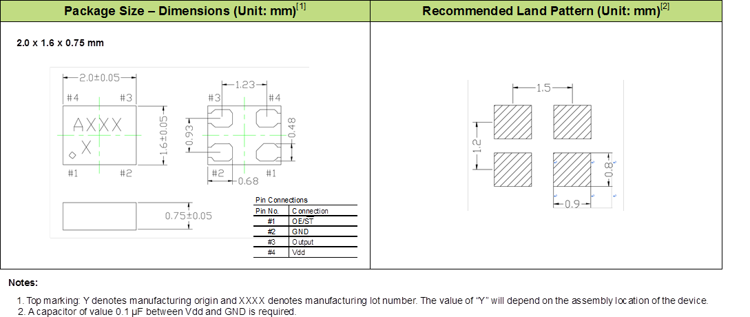
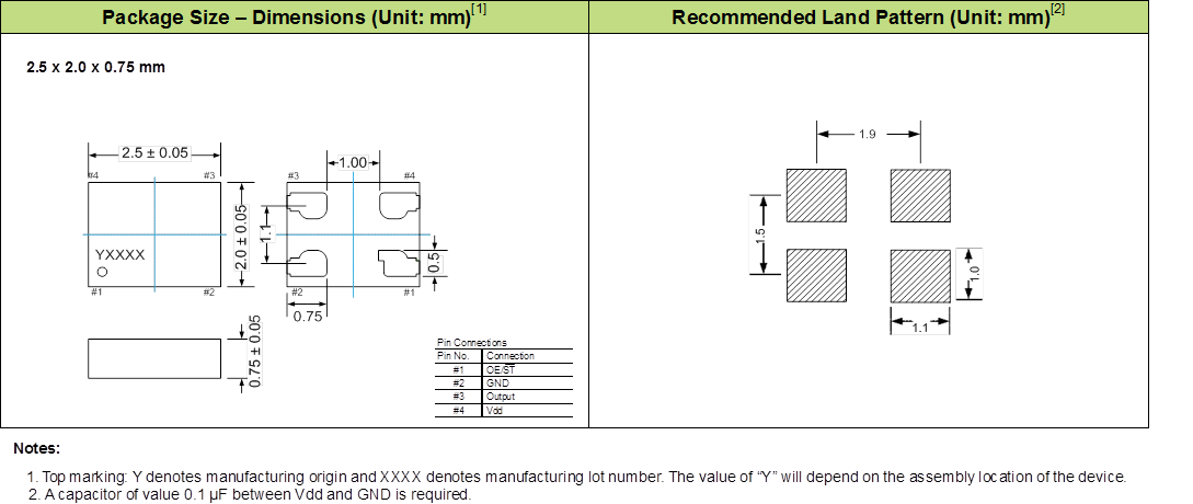
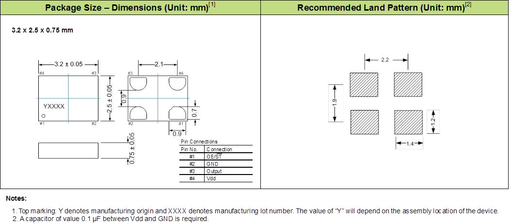
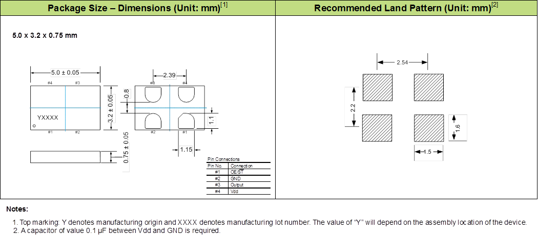
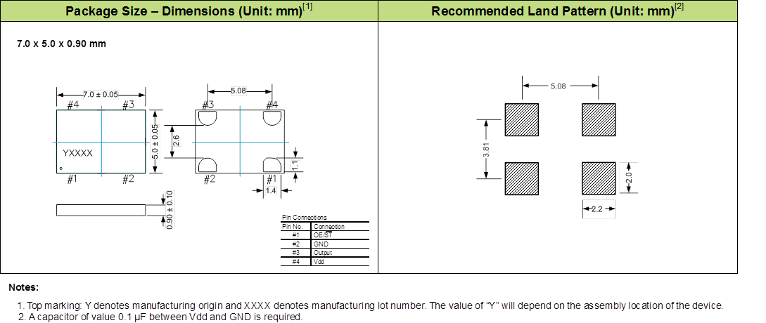
- Industry-standard packages: 2.0x1.6, 2.5x2.0, 3.2x2.5, 5.0x3.2, 7.0x5.0 mm
- Excellent total frequency stability as low as ±20 x 10-6
- Low power consumption of +3.5 mA typical at f = 20 MHz, Vdd = +1.8V
Applications
- Ideal for DSC, DVC, DVR, IP CAM, Tablets, e-Books, SSD, GPON, EPON, etc.
- Ideal for high-speed serial protocols such as: USB, SATA, SAS, Firewire,
100M / 1G / 10G Ethernet, etc.
Standard Specification
| Item | symbol | Min. | Typ. | Max. | Unit | Condition |
|---|---|---|---|---|---|---|
| Output Frequency Range | f | 3.57 | - | 77.76 | MHz | Refer to datasheet for exact list of supported frequencies |
| Supply Voltage | Vdd | +1.62 | +1.8 | +1.98 | V | |
| +2.25 | +2.5 | +2.75 | ||||
| +2.52 | +2.8 | +3.08 | ||||
| +2.7 | +3.0 | +3.3 | ||||
| +2.97 | +3.3 | +3.63 | ||||
| +2.25 | - | +3.63 | ||||
| Operating Temperature Range | T_use | -20 | - | +70 | ℃ | Extended Commercial |
| -40 | - | +85 | Industrial | |||
| Frequency STability | F_stab | -20 | - | +20 | ×10-6 | Inclusive of initial tolerance at +25℃, 1st year aging at +25℃, and variations over operating temperature, rated power supply voltage and load. |
| -25 | - | +25 | ||||
| -50 | - | +50 | ||||
| Current Consumption | Idd | - | +3.8 | +4.5 | mA | No load condition, f = 20 MHz, Vdd = +2.8V to +3.3V |
| - | +3.7 | +4.2 | No load condition, f = 20 MHz, Vdd = +2.5V | |||
| - | +3.5 | +4.1 | No load condition, f = 20 MHz, Vdd = +1.8V | |||
| OE Disable Current | I_od | - | - | +4.2 | mA | Vdd = +2.5V to +3.3V, OE = GND, Output is weakly pulled down |
| - | - | +4.0 | Vdd = +1.8V, OE = GND, Output is weakly pulled down | |||
| Standby Current | I_std | - | +2.6 | +4.3 | μA | ST= GND, Vdd = +2.8V to +3.3V, Output is weakly pulled down |
| - | +1.4 | +2.5 | ST= GND, Vdd = +2.5V , Output is weakly pulled down | |||
| - | +0.6 | +1.3 | ST= GND, Vdd = +1.8V, Output is weakly pulled down | |||
| Duty Cycle | DC | 45 | - | 55 | % | All Vdds |
| Output Low Voltage | VOL | - | - | Vdd × 0.1 | V | IOL = +4.0 mA (Vdd = +3.0V or +3.3V) IOL = +3.0 mA (Vdd = +2.8V and Vdd = +2.5V) IOL = +2.0 mA (Vdd = +1.8V) |
| Output High Voltage | VOH | Vdd × 0.9 | - | - | V | IOH = -4.0 mA (Vdd = +3.0V or +3.3V) IOH = -3.0 mA (Vdd = +2.8V and Vdd = +2.5V) IOH = -2.0 mA (Vdd = +1.8V) |
| Rise/Fall Time | Tr,Tf | - | 1.0 | 2.0 | ns | Vdd = +2.5V, +2.8V, +3.0V or +3.3V, 20% - 80% |
| - | 1.3 | 2.5 | Vdd =+1.8V, 20% - 80% | |||
| - | - | 2.0 | Vdd = +2.25V - +3.63V, 20% - 80% | |||
| Input Low Voltage | VIL | - | - | Vdd × 0.3 | V | Pin 1, OE or ST |
| Input High Voltage | VIH | Vdd × 0.7 | - | - | V | Pin 1, OE or ST |
| Start-up Time | T_start | - | - | 5.0 | ms | Measured from the time Vdd reaches its rated minimum value |
| Enable/Disable Time | T_oe | - | - | 138 | ns | f = 77.76 MHz. For other frequencies, T_oe = 100 ns + 3 * cycles |
| Resume Time | T_resume | - | - | 5.0 | ms | Measured from the time ST pin crosses 50% threshold |
| RMS Period Jitter | T_jitt | - | 1.8 | 3.0 | ps | f = 75 MHz, Vdd = +2.5V, +2.8V, +3.0V or +3.3V |
| - | 1.8 | 3.0 | f = 75 MHz, Vdd = +1.8V | |||
| Peak-to-peak Period Jitter | T_pk | - | 12 | 25 | ps | f = 75 MHz, Vdd = +2.5V, +2.8V, +3.0V or +3.3V |
| - | 14 | 30 | f = 75 MHz, Vdd = +1.8V | |||
| RMS Phase Jitter (random) | T_phj | - | 0.5 | 0.9 | ps | f = 75 MHz, Integration bandwidth = 900 kHz to 7.5 MHz |
| - | 1.3 | 2.0 | f = 75 MHz, Integration bandwidth = 12 kHz to 20 MHz |
Consult our sales representative for other specifications.
Dimentions, etc. (Click for full size)
Reference
TEL:+81-79-425-3141
FAX:+81-79-425-1134
FAX:+81-79-425-1134