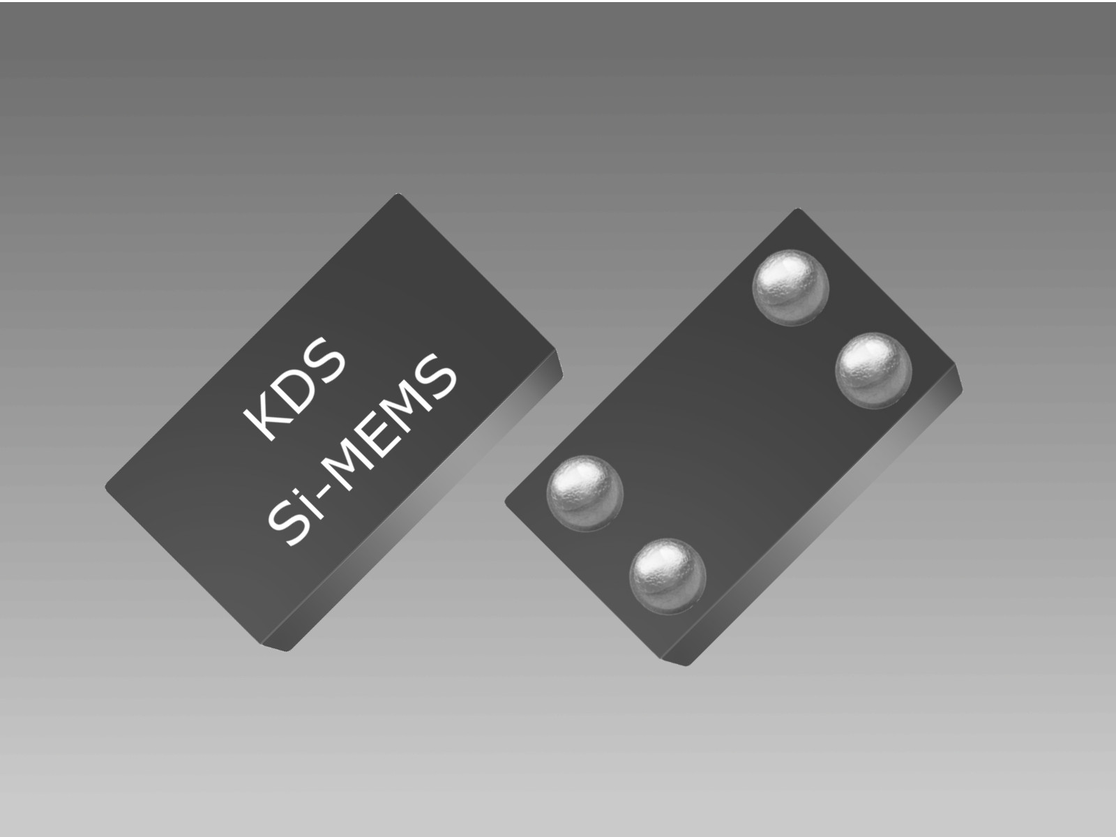
MO1532


Features
- Fixed 32.768 kHz
- Smallest footprint in chip-scale (CSP): 1.5 x 0.8 mm
- 10 x 10-6 frequency tolerance
- Ultra-low power: <+1 μA
- Internal filtering eliminates external Vdd bypass cap
- NanoDrive™ programmable output swing for lowest power
Applications
- Mobile Phones, Tablets
- Health and wellness monitors, Fitness Watches
- Pulse-per- second timekeeping, RTC reference clock
- Battery Management Timekeeping
Standard Specification
| Item | symbol | Min. | Typ. | Max. | Unit | Condition |
|---|---|---|---|---|---|---|
| Fixed Output Frequency | Fout | 32.768 | kHz | |||
| Operating Supply Voltage | Vdd | +1.2 | - | +3.63 | V | TA = -10°C to +70°C |
| +1.5 | - | +3.63 | TA = -40°C to +85°C | |||
| Operating Temperature Range | T_use | -10~+70 / -40~+85 | ℃ | |||
| Frequency stability [1] | F_stab | - | - | +75 | ×10-6 | TA = -10°C to +70°C, Vdd: +1.5V – +3.63V |
| - | - | +100 | TA = -40°C to +85°C, Vdd: +1.5V – +3.63V | |||
| - | - | +250 | TA = -10°C to +70°C, Vdd: +1.2V – +1.5V | |||
| Frequency Tolerance [2] | F_tol | - | - | +10 | ×10-6 | TA = +25°C, post reflow, Vdd: +1.5V – +3.63V. |
| - | - | +20 | TA = +25°C, post reflow with board-level underfill, Vdd: +1.5V – +3.63V | |||
| First yerar Frequency Aging | -1.0 | - | +1.0 | ×10-6 | TA = +25°C | |
| Core Operating Current [3] | Idd | - | +0.9 | - | μA | TA = +25°C, Vdd: +1.8V. No load |
| - | - | +1.3 | TA = -10°C to +70°C, Vdd max: +3.63V. No load | |||
| - | - | +1.4 | TA = -40°C to +85°C, Vdd max: +3.63V. No load | |||
| Start-up Time at Power-up [4] | T_start | - | 180 | 300 | ms | TA = -40°C ≤ TA ≤ +50°C, valid output |
| - | - | 450 | TA = +50°C < TA ≤ +85°C, valid output | |||
| LVCMOS Output Option, TA = -40°C to +85°C, typical values are at TA = +25°C | ||||||
| Output Clock Duty Cycle | DC | 48 | - | 52 | % | |
| Output Voltage Low | VOL | - | - | Vdd x 0.1 | V | Vdd: +1.5V – +3.63V, IOL = +10 μA, 15 pF |
| Output Voltage High | VOH | Vdd x 0.9 | - | - | V | Vdd: +1.5V – +3.63V, IOH = -10 μA, 15 pF |
| Output Rise/Fall Time | tr,tf | - | 100 | 200 | ns | 10-90% (Vdd), 15 pF load, Vdd = +1.5V to +3.63V |
| - | - | 50 | 10-90% (Vdd), 5 pF load, Vdd ≥ +1.62V | |||
| NanoDrive™ Programmable, Reduced Swing Output | ||||||
| Output Clock Duty Cycle | DC | 48 | - | 52 | % | |
| AC-coupled Programmable Output Swing | V_sw | - | +0.20 to +0.80 | - | MO1532 does not internally AC-couple. This output description is intended for a receiver that is AC-coupled. Vdd: +1.5V – +3.63V, 10 pF Load, IOH / IOL = ±0.2 μA | |
| DC-Biased Programmable Output Voltage Low Range | VOL | - | +0.35 to +0.80 | - | V | Vdd: +1.5V – +3.63V. IOL = +0.2 μA, 10 pF Load. |
| DC-Biased Programmable Output Voltage High Range | VOH | - | +0.60 to +1.225 | - | V | Vdd +1.5V – +3.63V. IOH = -0.2 μA, 10 pF Load. |
| Output Rise/Fall Time | Tr,Tf | - | - | 200 | ns | 30-70% (VOL/VOH), 10 pF Load |
| Packing Unit | 1000pcs./reel(φ180)or 3000pcs./reel(φ180) | |||||
[1]. Measured peak-to-peak. Inclusive of Initial Tolerance at +25°C, and variations over operating temperature, rated power supply voltage and load.
Stability is specified for two operating voltage ranges. Stability progressively degrades with supply voltage below +1.5V.
[2]. Measured peak-to-peak. Tested with Keysight 53132A frequency counter.
Due to the low operating frequency, the gate time must be ≥100 ms to ensure an accurate frequency measurement.
[3]. Core operating current does not include output driver operating current or load current. To derive total operating current (no load),
add core operating current + (+0.065 μA/V) * (output voltage swing).
[4]. Measured from the time Vdd reaches +1.5V
Consult our sales representative for other specifications.
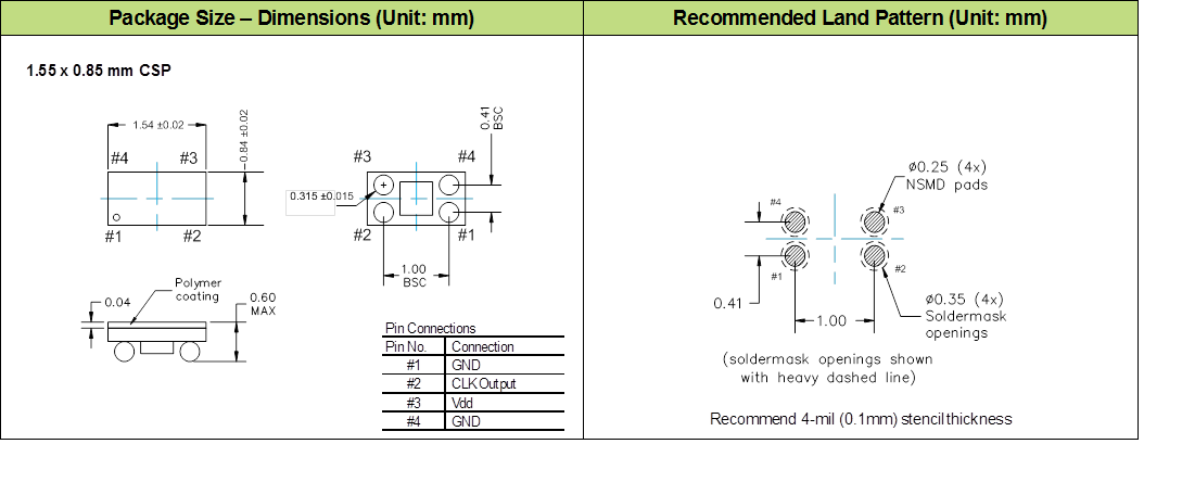
Dimentions, etc. (Click for full size)
Reference
FAX:+81-79-425-1134