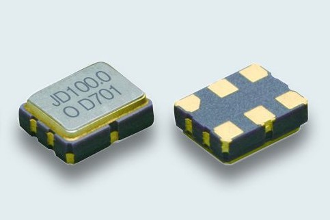
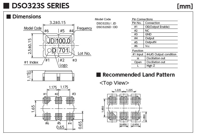
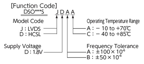
DSO323SD


Features
- 1.8V operating voltage, High speed type
- 3-state function
- HCSL output
- AEC-Q200 Compliant (Option: Equivalent to AEC-Q100)
Applications
- Sever, Optical transmission device, Communication base station and Automotive multimedia device
Standard Specification
| Type | Legend | DSO323SD |
|---|---|---|
| Output Specification | - | HCSL |
| Output Frequency Range | fo | 27 to 100MHz |
| Supply Voltage | VCC | +1.8V±0.09V |
| Frequency Tolerance (Includes frequency tolerance at room temperature.) |
f_tol | ±50×10-6 max., ±100×10-6 max. |
| Storage Temperature Range | T_stg | -40 to +85℃ |
| Operating Temperature Range | T_use | -10 to +70℃, -40 to +85℃ |
| Current Consumption | ICC | 25mA max. |
| Stand-by Current (#1 pin "L" Level) | I_std | 10μA max. |
| Load Condition | Load-R | 50Ω |
| Symmetry | SYM | 45 to 55% [at outputs cross point] |
| 0 Level Output Voltage | VOL | -0.15 to 0.15V |
| 1 Level Output Voltage | VOH | 0.50 to 1.0V |
| Rise and Fall Time | tr, tf | 0.6ns max. [20 to 80%Vopp] |
| Differential Output Voltage | VOD1, VOD2 | - |
| Change to VOD | ΔVOD | - |
| Offset Voltage | VOS | - |
| Offset to VOS | ΔVOS | - |
| OE Pin 0 Level Input Voltage | VIL | VCC×0.3 max. |
| OE Pin 1 Level Input Voltage | VIH | VCC×0.7 min. |
| Output Disable Time | tPLZ | 200ns |
| Output Enable Time | tPZL | 2ms |
| Period Jitter (1) | tRMS | 2.5ps typ. (σ) |
| tp-p | 22ps typ. (Peak to peak) | |
| Total Jitter (1) | tTL | 35ps typ. [tDJ + n×tRJ n=14.1 (BER=1×10-12) (2)] |
| Phase Jitter | tpj | 1ps max. |
| Packing Unit (3) | - | 2000pcs./reel (Φ180) |
(1) Measured WAVECREST DTS-2075
(2) tDJ: Deterministic jitter tRJ: Random jitter
(3) Moisture prevention packing is unnecessary.
Moisture Sensitivity Level: LEVEL 1(IPC/JEDEC J-STD-033)
Consult our sales representative for other specifications.
Dimentions, etc. (Click for full size)
Reference
TEL:+81-79-425-3141
FAX:+81-79-425-1134
FAX:+81-79-425-1134