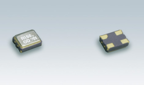
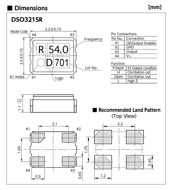
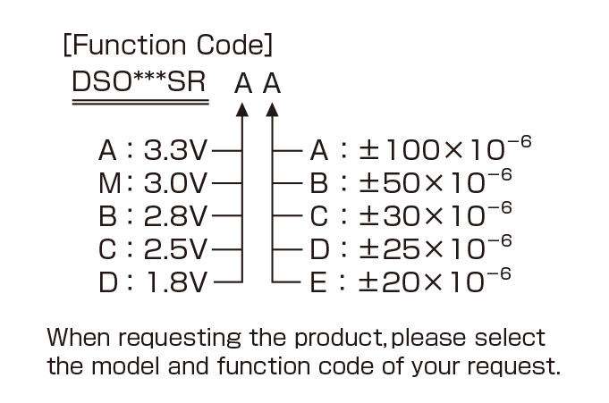
DSO321SR


Features
- Low current consumption: 8mA max (167MHz, 3.3V)
- Supply Voltage: 1.8V/2.5V/2.8V/3.0V/3.3V
- Offers Narrow deviation: ±20×10-6/±30×10-6/±50×10-6/±100×10-6
- Available up to 167MHz by using AT cut fundamental resonator. Low jitter provides for high performance.
- Low profile: 1.1mm
- AEC-Q200 Compliant (Option: Equivalent to AEC-Q100)
- CMOS Level Output
Applications
- PC, Gaming equipment
- DSC, DVD, Blu-ray, HDTV, DVC, HDD
- WiMAX
- Camera module
- GbEthernet
- Automotive multimedia device
Standard Specification
| Item | Function Code | Output Frequency Range (MHz) |
Legend | Spec. | Condition | |||||
|---|---|---|---|---|---|---|---|---|---|---|
| Supply Voltage |
Frequency tolerance |
min. | typ. | max. | Unit | |||||
| Supply Voltage | A | * | 0.2≦fo≦167 | VCC | +3.0 | +3.3 | +3.6 | V | ||
| M | 0.2≦fo≦167 | +2.7 | +3.0 | +3.3 | ||||||
| B | 0.2≦fo≦157 | +2.6 | +2.8 | +3.0 | ||||||
| C | 0.2≦fo≦157 | +2.25 | +2.5 | +2.75 | ||||||
| D | 0.2≦fo≦80 | +1.6 | +1.8 | +2.0 | ||||||
| Frequency Tolerance (Includes frequency tolerance at room temperature.) |
* | A | 0.2≦fo≦167 | f_tol | -100 | - | +100 | ×10-6 | -40 to +85℃ | -10 to +70℃ (Standard Operating Temperature Range) |
| B | 0.2≦fo≦125 | -50 | - | +50 | ||||||
| C | 0.2≦fo≦80 | -30 | - | +30 | -20 to +70℃ | |||||
| D | 0.2≦fo≦80 | -25 | - | +25 | ||||||
| E | 0.2≦fo≦50 | -20 | - | +20 | -10 to +70℃ | |||||
| Current Consumption | A, M | * | 0.2≦fo<32 | ICC | - | - | 1.8 | mA | No Load | |
| 32≦fo<54 | - | - | 2.5 | |||||||
| 54≦fo<80 | - | - | 5.0 | |||||||
| 80≦fo<125 | - | - | 6.0 | |||||||
| 125≦fo≦167 | - | - | 8.0 | |||||||
| B | * | 0.2≦fo<32 | - | - | 1.8 | |||||
| 32≦fo<54 | - | - | 2.5 | |||||||
| 54≦fo<125 | - | - | 5.0 | |||||||
| 125≦fo≦157 | - | - | 7.0 | |||||||
| C | * | 0.2≦fo<32 | - | - | 1.5 | |||||
| 32≦fo<54 | - | - | 2.0 | |||||||
| 54≦fo<125 | - | - | 4.0 | |||||||
| 125≦fo≦157 | - | - | 6.0 | |||||||
| D | * | 0.2≦fo<32 | - | - | 1.0 | |||||
| 32≦fo<54 | - | - | 1.4 | |||||||
| 54≦fo≦80 | - | - | 3.0 | |||||||
| Stand-by Current (#1 pin "L" Level) |
* | * | * | I_std | - | - | 10 | μA | ||
| Load Condition | * | * | * | L_CMOS | - | - | 15 | pF | ||
| A, M | 0.2≦fo≦80 | - | - | 30 | ||||||
| Symmetry | * | * | fo<50 | SYM | 45 | 50 | 55 | % | 50% VCC Level | |
| fo≧ 50 | 40 | 50 | 60 | |||||||
| 0 Level Output Voltage | * | * | * | VOL | - | - | VCC×0.1 | V | ||
| 1 Level Output Voltage | * | * | * | VOH | VCC×0.9 | - | - | |||
| Rise and Fall Time | A, M, B, C | * | 0.2≦fo≦54 | tr, tf | - | - | 5 (4) | ns | L_CMOS:15pF 10 to 90% VCC Level (20 to 80% VCC Level) |
|
| D | 0.2≦fo≦54 | - | - | 7 (6) | ||||||
| * | 54<fo<100 | - | - | 4 (3) | ||||||
| * | 100≦fo≦167 | - | - | 3 (2.5) | ||||||
| A, M | 0.2≦fo≦54 | - | - | 10 | L_CMOS:30pF 10 to 90% VCC Level | |||||
| A, M | 54<fo≦80 | - | - | 6 | ||||||
| OE Pin 0 Level Input Voltage | * | * | * | VIL | - | - | VCC×0.2 | V | ||
| OE Pin 1 Level Input Voltage | * | * | * | VIH | VCC×0.8 | - | - | |||
| Output Disable Time | * | * | * | tPLZ | - | - | 150 | ns | ||
| Output Enable Time | * | * | * | tPZL | - | - | 1 | ms | ||
| Period Jitter (1) | * | * | * | tRMS | - | 2.2 | - | ps | σ | |
| tp-p | - | 20 | - | Peak to peak | ||||||
| Total Jitter (1) | * | * | * | tTL | - | 31 | - | ps | tDJ+n×tRJ n=14.1 (BER=1×10-12) (2) | |
| Phase Jitter | * | * | 40≦fo≦167 | tpj | - | - | 1 | ps | fo offset:12kHz to 20MHz | |
| 10≦fo<40 | fo offset:12kHz to 5MHz | |||||||||
| Packing Unit (3) | 2000pcs./reel (Φ180) | |||||||||
(1) Measured WAVECREST DTS-2075
(2) tDJ: Deterministic jitter tRJ: Random jitter
(3) Moisture prevention packing is unnecessary.
Moisture Sensitivity Level: LEVEL1(IPC/JEDEC J-STD-033)
Consult our sales representative for other specifications.
Dimentions, etc. (Click for full size)
Reference
TEL:+81-79-425-3141
FAX:+81-79-425-1134
FAX:+81-79-425-1134