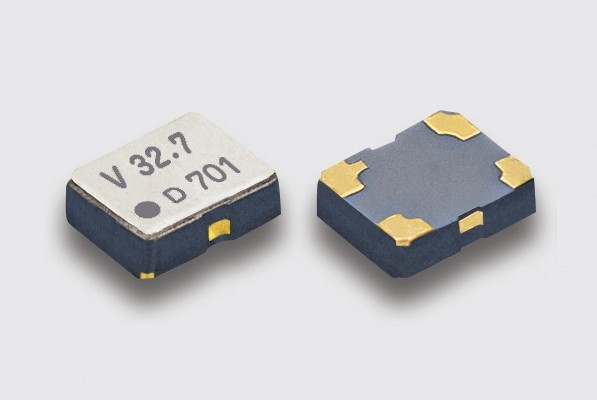
DSK1612ATD


优点
- 数字温度补偿类型
- 高精度:±5.0×10⁻⁶(-40~85℃)
- 低消耗电流
- CMOS输出
用途
- 时钟用高精度标准
- RTC用高精度标准
一般规格
| 项 目 | 符号 | 规格值 | 条 件 | |||
|---|---|---|---|---|---|---|
| min. | typ. | max. | Unit | |||
| 输出频率 | fo | - | 32.768 | - | kHz | |
| 电源电压范围 | VCC | +1.5 | - | +3.63 | V | 温度补偿运行 |
| 频率公差 (含常温偏差) |
f_tol | -5.0 | - | +5.0 | ×10-6 | -40〜+85℃ |
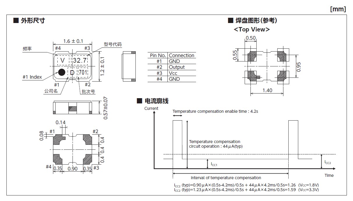
| 消耗电流 | ICC1 | - | 0.90 | 1.90 | μA | VCC=+1.8V, TA=-40~+85℃, at No Load (1) |
| - | 1.23 | 2.60 | VCC=+3.3V, TA=-40~+85℃, at No Load (1) | |||
| ICC2 | - | 1.26 | 2.43 | VCC=+1.8V, TA=-40~+85℃, at No Load Temperature Compensation Interval: 0.5s (standard specification) (2) |
||
| - | 1.59 | 3.12 | VCC=+3.3V, TA=-40~+85℃, at No Load Temperature Compensation Interval: 0.5s (standard specification) (2) |
|||
| 波形対称性 | SYM | 40 | 50 | 60 | % | at 50% VCC |
| 0电平电压 | VOL | - | - | VCC×0.1 | V | |
| 1电平电压 | VOH | VCC×0.9 | - | - | ||
| 上升时间 下降时间 |
tr, tf | - | - | 40 | ns | 10〜90% VCC Level |
| 输出负载条件 | L_CMOS | - | - | 15 | pF | |
| 启动时间 | Tstart | - | - | 0.5 | s | |
| 包装单位(3) | 3000pcs./reel (φ180) | |||||
(1)ICC1 是关闭温度补偿电路时的电流值
(2)ICC2 是温度补偿电路的开起状态和关闭状态的平均电流值
(3)无需防湿包装管理 Moisture Sensitivity Level: Level1 (IPC/JEDEC J-STD-033)
有关其他规格或者特殊规格请咨询营业部门。
外形尺寸等 (点击看大图)
参考
TEL:+81-79-425-3141
FAX:+81-79-425-1134
FAX:+81-79-425-1134