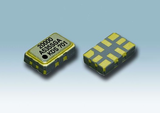
DSB535SGA


Features
- 5032 size, 1.35mm height.
- Ultra high precision SMD TCXO
- Clipped sine output or CMOS level output
- Low phase noise
- Single packaged structure
Applications
- Stratum3, 5G compatible devices, Networking, Base station
Standard Specification
| Item | DSB535SGA(VC-TCXO) | ||
|---|---|---|---|
| Output Frequency Range | 10 to 52MHz | ||
| Standard Frequency | 10MHz/ 19.2MHz/ 20MHz/ 38.88MHz | ||
| Supply Voltage (Range) | +2.3 to +3.63V | ||
| Supply Voltage (VCC) | +2.8V/ +3.0V/ +3.3V | ||
| Current Consumption | +4.0mA max. (Clipped sine)/ +8.0mA・max. (CMOS) | ||
| Output Level | 0.8Vp-p min.(Clipped sine/ DC-coupled) '0'level 0.1×VCC V max./ '1'level 0.9×VCC V min. (CMOS) |
||
| Output Load | 10kΩ//10pF (Clipped sine)/ 15pF (CMOS) | ||
| Frequency Stability | Tolerance | ±1.5×10⁻⁶ max.(After 2 reflows) | |
| vs. Temperature | ±0.10×10⁻⁶ max./ -40 to +85℃ ±0.20×10⁻⁶ max./ -40 to +105℃ |
||
| vs. Hysteresis | ±0.10×10⁻⁶ max. | ||
| vs. Supply Votage | ±0.1×10⁻⁶ max. (VCC±5%: Clipped sine, CMOS (40MHz≦f))/ ±0.2×10⁻⁶ max. (VCC±5%: CMOS (40MHz<f)) | ||
| vs. Load Variation | ±0.20×10⁻⁶ max.(10kΩ//10pF±10%/ 15pF±10%) | ||
| vs. Aging | ±1.0×10⁻⁶ max./year | ||
| Total Frequency Tolerance | ±4.6×10⁻⁶ max. (Inclusive of variations over operating temperature, initial tolerance, supply voltage, load variation, aging) | ||
| Phase Noise Offset 100Hz Offset 1kHz Offset 10kHz Offset 100kHz |
20MHz(typ.) -118dBc/Hz -139dBc/Hz -155dBc/Hz -158dBc/Hz |
||
| Packing Unit (1) | 1000pcs./reel(φ180),4000pcs./reel(φ330) | ||
(1) Moisture prevention packing is unnecessary.
Moisture Sensitivity Level: LEVEL 1 (IPC/JEDEC J-STD-033)
Consult our sales representative for other specifications.
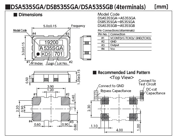
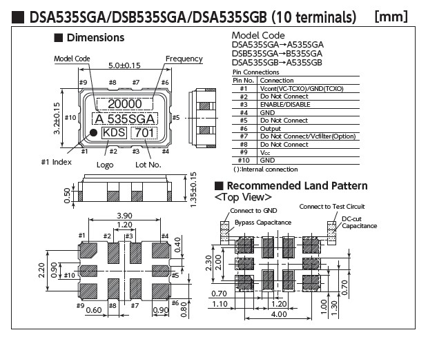
Dimentions, etc. (Click for full size)
Reference
TEL:+81-79-425-3141
FAX:+81-79-425-1134
FAX:+81-79-425-1134