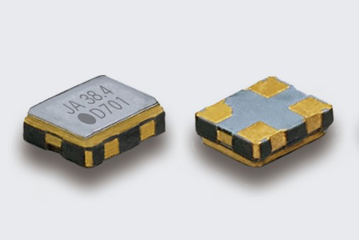
DSB211SJA


Features
- Capable of operating over a wide temperature range, from -40 to +105℃
- Supply voltage up to +1.7 to +3.6V
- Clipped sine output or CMOS level output
- Low phase noise
- Single package structure
- AEC-Q100/AEC-Q200 Compliant
Applications
- Automotive multimedia device, WiLAN and visual applications such as automotive camera
Standard Specification
| Type | DSB211SJA (TCXO) | |||
|---|---|---|---|---|
| Frequency Range | 13 to 54MHz | |||
| Standard Frequency | 19.2MHz/ 25MHz/ 26MHz/ 32MHz/ 38.4MHz/ 40MHz/ 48MHz/ 52MHz | |||
| Supply Voltage (VCC) | +1.8V/ +2.5V/ +2.8V/ +3.3V | |||
| Current Consumption | +3.0mA max. (Clipped sine) +5.0mA max. [No Load] (CMOS) |
|||
| Stand-by Current (#1 pin "L" Level) |
+10μA max. | |||
| Frequency Stability | Tolerance | ±1.5×10⁻⁶ max. (After 2 reflows) | ||
| vs. Temperature | ±2.5×10⁻⁶ max./ -30 to +85℃ ±5.0×10⁻⁶ max./ -40 to +105℃ ±20×10-6 max./ -40 to +125℃ (Option) |
|||
| vs. Aging | ±1.0×10⁻⁶ max. /year | |||
| Symmetry | 45 to 55% (GND Level [DC cut]) (Clipped sine) 45 to 55% (50% VCC Level) (CMOS) |
|||
| 0 Level Output Voltage | VCC×0.1V max. | |||
| 1 Level Output Voltage | VCC×0.9V min. | |||
| Output Load | 10kΩ//10pF (Clipped sine) 15pF (CMOS) |
|||
| Rise and Fall Time | − (Clipped sine) 5ns max. (10% to 90% VCC Level) (CMOS) |
|||
| OE Pin 0 Level Input Voltage | VCC×0.2V max. | |||
| OE Pin 1 Level Input Voltage | VCC×0.8V min. | |||
| Start Up Time | 3.0ms max. | |||
| Output Enable Time | 3.0ms max. | |||
| Output Disable Time | 150ns max. | |||
| Phase Noise Offset 1kHz Offset 100kHz |
[f≦26MHz] -145dBc/Hz -158dBc/Hz |
[26MHz<f≦52MHz] -141dBc/Hz -157dBc/Hz |
||
| Reliability | AEC-Q100/AEC-Q200 | |||
| Packing Unit (1) | 3000pcs./reel (φ180) | |||
(1) Moisture prevention packing is unnecessary.
Moisture Sensitivity Level: LEVEL 1(IPC/JEDEC J-STD-033)
Consult our sales representative for other specifications.
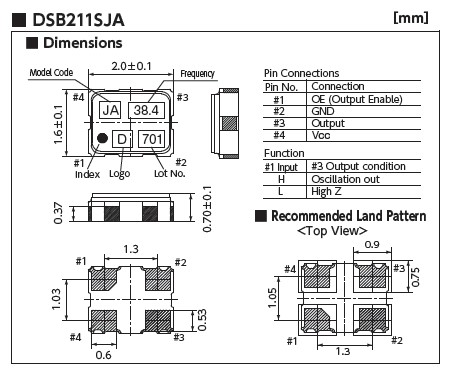
Dimentions, etc. (Click for full size)
Reference
TEL:+81-79-425-3141
FAX:+81-79-425-1134
FAX:+81-79-425-1134