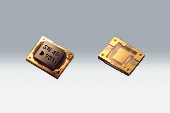
DS1008JN (Arkh.3G)


Features
- 1008 size, height 0.22mm max.
Unprecedented extremely low-profile package using a novel structure - Available frequency range: 1 to 100MHz
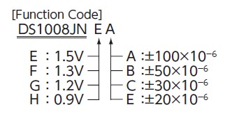
- Low Supply Voltage: 0.9V/ 1.2V/ 1.3V/ 1.5V typ
- 3-state function
- CMOS level output
- Available up to 100MHz by using AT cut fundamental resonator.
Low jitter provides for high performance
Applications
- Medical camera
- Wearable devices
- IoT devices
- Multimedia device
Standard Specification
| Item | Function Code | Output Frequency Range (MHz) | Legend | Spec. | Condition | |||||
|---|---|---|---|---|---|---|---|---|---|---|
| Supply Voltage | Frequency Tolerance | min. | typ. | max. | Unit | |||||
| Supply Voltage | E | * | 1≦f0≦100 | Vcc | 1.4 | 1.5 | 1.6 | V | ||
| F | 1.2 | 1.3 | 1.4 | |||||||
| G | 1.1 | 1.2 | 1.3 | |||||||
| H | 0.8 | 0.9 | 1.0 | |||||||
| Frequency Tolerance (Includes frequency tolerance at room temperature.) |
* | A | * | f_tol | - | - | ±100 | ×10-6 | -40 to +125℃ | -20 to +70℃ (Standard Operating Temperature Range) |
| B | - | - | ±50 | |||||||
| C | - | - | ±30 | -30 to +85℃ | ||||||
| E | - | - | ±20 | -20 to +70℃ | ||||||
| Current Consumption | E | * | 80≦fo≦100 | ICC | - | - | 3.1 | mA | No Load | |
| 50≦fo<80 | - | - | 2.7 | |||||||
| 1≦fo<50 | - | - | 2.2 | |||||||
| F | * | 80≦fo≦100 | - | - | 2.8 | |||||
| 50≦fo<80 | - | - | 2.5 | |||||||
| 1≦fo<50 | - | - | 2.1 | |||||||
| G | * | 80≦fo≦100 | - | - | 2.7 | |||||
| 50≦fo<80 | - | - | 2.4 | |||||||
| 1≦fo<50 | - | - | 2.0 | |||||||
| H | * | 80≦fo≦100 | - | - | 2.3 | |||||
| 50≦fo<80 | - | - | 2.1 | |||||||
| 1≦fo<50 | - | - | 1.8 | |||||||
| Stand-by Current (#1 pin "L" Level) |
* | * | * | I_std | - | - | 0.02 | mA | ||
| Load Condition | * | * | * | L_CMOS | - | - | 15 | pF | ||
| Symmetry | * | * | * | SYM | 40 | 50 | 60 | % | at 50% | |
| Rise and Fall Time | * | * | * | tr, tf | - | - | 5 | ns | 10 to 90% VCC Level | |
| Output Enable Time | * | * | * | tPZL | - | - | 2 | ms | ||
| Output Disable Time | * | * | * | tPLZ | - | - | 200 | ns | ||
| OE Pin 1 Level Input Voltage | * | * | * | VIH | VCC × 0.8 | - | - | V | ||
| OE Pin 0 Level Input Voltage | * | * | * | VIL | - | - | VCC × 0.2 | V | ||
| Packing Unit (1) | 3000pcs./reel (φ180) | |||||||||
(1) Moisture prevention packing
Consult our sales representative for other specifications.
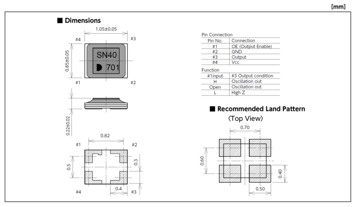
Dimentions, etc. (Click for full size)
Reference
TEL:+81-79-425-3141
FAX:+81-79-425-1134
FAX:+81-79-425-1134