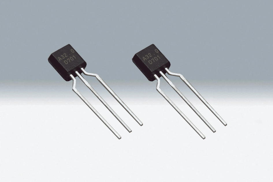
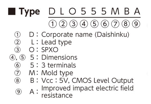
DLO555MBA


Features
- Small crystal oscillator in TO92 package
- Built-in bypass capacitor to improve noise resistance
- No PLL, No multiplier in oscillation circuit (The divider circuit, some cases be used)
- High-speed oscillation start up time (1ms)
- CMOS Level Output
Applications
- Gaming equipment
- Industrial equipment
Absolute Maximum Ratings
| Item | Legend | Spec. | Unit |
|---|---|---|---|
| Supply Voltage | Vcc | -0.5 to +6.0 | V |
| Output Pin Voltage | VOUT | -0.5 to Vcc+0.5 | V |
| Output Pin Current | IOUT | 10 | mA |
| Storage Temperature Range | T_str | -40~+105 | ℃ |
Recommended Operating Conditions
| Item | Legend | min. | typ. | max. | Unit |
|---|---|---|---|---|---|
| Supply Voltage | Vcc | 3.0 | 5.0 | 5.5 | v |
| Load Condition | L_CMOS | - | - | 15 | pF |
| 30 | |||||
| Operating Temperature Range | T_opr | -10 | - | +85 | ℃ |
Standard Specification
| Item | Legend | Spec. | Unit | Condition | ||
|---|---|---|---|---|---|---|
| min. | typ. | max. | ||||
| Output Frequency Range | fo | 1.5 | - | 54 | MHz | L_CMOS: 30pF |
| Frequency Tolerance | - | -100 | - | +100 | ×10-6 | T_opr=-10〜+85℃ VCC=+3.0 to +5.5V |
| -50 | +50 | |||||
| Aging | - | - | - | ±5 | ×10-6/year | |
| Current Consumption | ICC | - | - | 8 | mA | No load |
| Symmetry | SYM | 45 | - | 55 | % | 50% VCC level |
| 0 Level Output Voltage | VOL | - | - | VCC×0.1 | V | |
| 1 Level Output Voltage | VOH | VCC×0.9 | - | - | V | |
| Rise and Fall Time | tr,tf | - | - | 7.5 | ns | L_CMOS: 30pF 20 to 80% VCC level |
| Start Up Time | T_start | - | - | 1 | ms | t=0 at 90% VCC |
| Phase Noise | - | - | -139 | - | dBc/Hz | Offset 1kHz |
| - | -156 | - | Offset 100kHz | |||
| Period Jitter (1) | tRMS | - | 2.4 | - | ps | σ |
| tp-p | - | 20 | - | Peak to peak | ||
| Total Jitter (1) | tTL | - | 34 | - | tDJ+n×tRJ n=14.1 (BER=1×10-12) (2) | |
| Phase Jitter (3) | tpj | - | - | 1 | 10MHz≦fo<40MHz fo offset12kHz to 5MHz | |
| 40MHz≦fo≦54MHz fo offset12kHz to 20MHz | ||||||
| Built-in Bypass Capacitors Capacitance | Cbp | - | 0.1 | - | μF | VCC to GND capacitance |
(1) Measured WAVECREST DTS-2075
(2) tDJ: Deterministic jitter tRJ: Random jitter
(3) Measured Keysight Technologies E5052B
*Moisture prevention packing is unnecessary. Moisture Sensitivity Level: Level1 (IPC/JEDEC J-STD-033)
Consult our sales representative for other specifications.
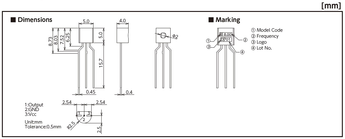
Dimentions, etc. (Click for full size)
Reference
TEL:+81-79-425-3141
FAX:+81-79-425-1134
FAX:+81-79-425-1134