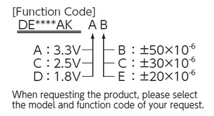
DE3225AJ (Arkh.2G)


Features
- Available frequency: 100MHz, 125MHz, 156.25MHz, 312.5MHz
- Supports a wide operating temperature range with narrow tolerance from −40 to +105℃
- LVDS output
- AEC-Q200 Compliant (Option: Equivalent to AEC-Q100)
Applications
- Optical transceiver, Optical transmission device, Communication base station, Automotive multimedia device
Standard Specification
| Type | Legend | DE3225AJ |
|---|---|---|
| Output Specification | - | LVDS |
| Output Frequency Range | fo | 100MHz/125MHz/156.25MHz/312.5MHz |
| Supply Voltage | VCC | +1.8±0.090V/+2.5±0.125V/+3.3±0.165V |
| Frequency Tolerance (Includes frequency tolerance at room temperature.) | f_tol | ±30×10-6 max., ±50×10-6 max. (Option ±20×10-6 max.) |
| Storage Temperature Range | T_stg | -40 to +125℃ |
| Operating Temperature Range | T_use | -40 to +85℃, -40 to +105℃ |
| Current Consumption | ICC | 23mA max. (156.25MHz), 38mA max. (312.5MHz) |
| Stand-by Current (#1 pin "L"Level) | I_std | 60μA max. |
| Load Condition | Load-R | 100Ω Output-OutputN |
| Symmetry | SYM | 45 to 55% [1/2VOPP] |
| 0 Level Output Voltage | VOL | - |
| 1 Level Output Voltage | VOH | - |
| Rise and Fall Time | tr, tf | 0.35ns max. [20 to 80% VOPP] |
| Output Voltage | VOPP | 0.5V min. |
| Differential Output Voltage | VOD1, VOD2 | 0.25 to 0.45V (Option:0.30 to 0.60V, 0.40 to 0.80V) |
| Change to VOD | ΔVOD | 50mV [⊿VOD=|VOD1-VOD2|] |
| Offset Voltage | VOS | 0.65 to 0.85V (+1.8V), 1.125 to 1.375V (+2.5V, +3.3V) |
| Offset to VOS | ΔVOS | 50mV |
| OE Pin 0 Level Input Voltage | VIL | VCC×0.2 max. |
| OE Pin 1 Level Input Voltage | VIH | VCC×0.8 min. |
| Output Disable Time | tPLZ | 100ns max. |
| Output Enable Time | tPZL | 500ns max. |
|
Phase Jitter |
tpj | 40fs typ., 80fs max. (156.25MHz/VCC=+2.5V, +3.3V) 32fs typ., 60fs max. (312.5MHz/VCC=+2.5V, +3.3V) |
| Packing Unit (1) | - | 2000pcs./reel (Φ180) |
(1) Moisture prevention packing is unnecessary.
Moisture Sensitivity Level: LEVEL 1(IPC/JEDEC J-STD-033)
Consult our sales representative for other specifications.
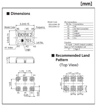
Dimentions, etc. (Click for full size)
Reference
TEL:+81-79-425-3141
FAX:+81-79-425-1134
FAX:+81-79-425-1134