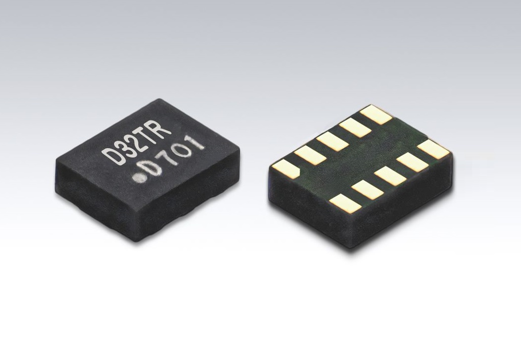
DD3225TR


Features
- Precision: ±11.5×10⁻⁶ (30 seconds per month),
±23.0×10⁻⁶ (60 seconds per month) - Low current consumption
- Low voltage operation: +1.5 to +5.5V, +1.3 to +5.5V (Clock Timing
Operating) - I2C-BUS serial interface: 400kHz fast-mode compatible
- Clock function: hour・minute・second,Calendar function with auto
leap year adjustment: year・month・day・day of week - Alarm interrupt function: day・day of week・hour・minute
- Fixed-cycle timer interrupt function: 244.14μs to 255min
- Time update interrupt function: minute・second
- Clock output function: 32.768kHz, 1024Hz, 32Hz, 1Hz
- Supply voltage detection function: +1.5V temperature compensation operating
voltage detection, +1.3V supply voltage under voltage detection - CMOS Level Output
"I2C-BUS" is a trademark of NXP semiconductors.
Applications
- Calendar, Timer, Alarm, Standard for watches
- Remote control with calendar, Data logger, Wireless sensor, Amusement device
Standard Specification
| Item | Legend | Spec. | unit | Condition | |||
|---|---|---|---|---|---|---|---|
| min. | typ. | max. | |||||
| Output Frequency | fo | - | 32.768 | - | kHz | ||
| Supply Voltage Range | VCC | +1.3 | - | +5.5 | V | (Clock Timing Operating) | |
| Vint | +1.5 | - | +5.5 | (Interface Operation) I2C-BUS | |||
| Frequency Tolerance | f_tol | -11.5 | - | +11.5 | ×10-6 | Ta=25℃, Vcc=+3.0V (30 seconds per month) | |
| -23 | - | +23 | Ta=25℃, Vcc=+3.0V (60 seconds per month) | ||||
| Operating temperature range | Ta | -40 | - | +85 | ℃ | ||
| Current Consumption | ICC1 | - | 0.29 | 2.10 | μA | VCC=+3.0V | SCL=SDA=INTN=Vcc,OE=GND (Output Off) |
| - | 0.41 | 2.90 | VCC=+5.0V | ||||
| ICC2 | - | 0.89 | 2.80 | VCC=+3.0V | No Load, SCL=SDA=INTN=OE=Vcc (Output On) |
||
| - | 1.29 | 4.00 | VCC=+3.0V | ||||
| Load Condition | L_CMOS | - | - | 15 | pF | ||
| Symmetry | SYM | 40 | - | 60 | % | 50%VCC | |
| 1 level Output Voltage | VOH | 0.8×Vcc | - | - | V | IOH=-1mA | |
| 0 level Output Voltage | VOL | - | - | 0.2×Vcc | V | IOL=1mA | |
| Rise / Fall Time | Tr/Tf | - | - | 100 | ns | 20 to 80%Vcc | |
| OE Pin 1 level Input Voltage |
VIH | 0.8×Vcc | - | Vcc | V | ||
| OE Pin 0 level Input Voltage |
VIL | 0 | - | 0.2×Vcc | V | ||
| Start Up Time | Tstart | - | - | 1 | s | Ta=+25℃, Vcc=+1.3V | |
| Packing Unit (1) | 2000pcs./reel(φ180) | ||||||
(1) Moisture prevention packing
Moisture sensitivity level: Level 2 (IPC/JEDEC J-STD-033)
Consult our sales representative for other specifications.
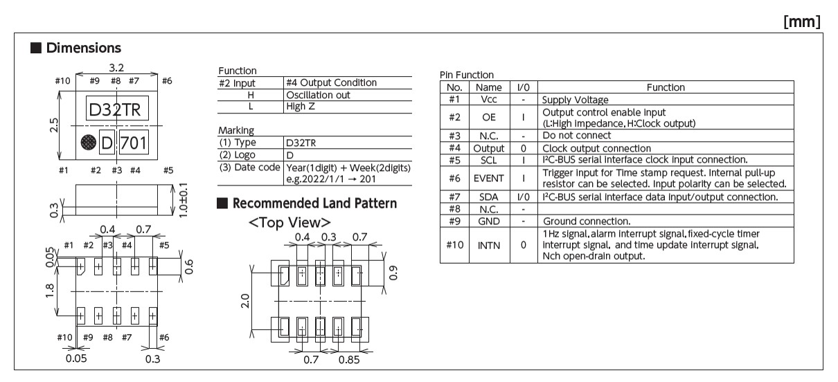
Pin Function
| No. | Name | I/O | Function |
|---|---|---|---|
| #1 | Vcc | - | Supply Voltage |
| #2 | OE | I | Output control enable input (L: High impedance,H: Clock output) |
| #3 | N.C. | - | Do not connect |
| #4 | Output | O | Clock output connection |
| #5 | SCL | I | I2C-BUS serial interface clock input connection |
| #6 | EVENT | I | Trigger input for Time stamp request. Internal pull-up resistor can be selected. Input polarity can be selected. |
| #7 | SDA | I/O | I2C-BUS serial interface data input/output connection |
| #8 | N.C. | - | Do not connect |
| #9 | GND | - | Ground connection |
| #10 | INTN | O | 1Hz signal,alarm interrupt signal,fixed-cycle timer interrupt signal, and time update interrupt signal, Nch open-drain output. |
Dimentions, etc. (Click for full size)
Reference
TEL:+81-79-425-3141
FAX:+81-79-425-1134
FAX:+81-79-425-1134