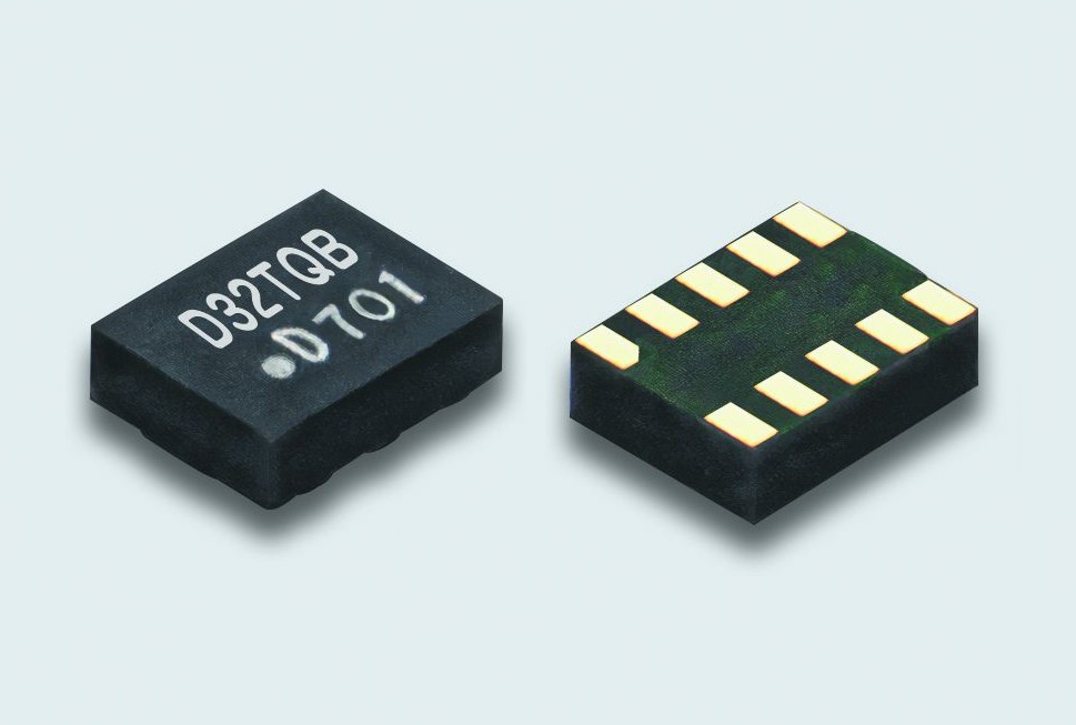
DD3225TQB


优点
- Digital temperature compensated type
- Low current consumption
- High precision: ±5.0×10⁻⁶ (-40 to +85℃), ±8.0×10⁻⁶ (+85 to +105℃)
- I2C-BUS serial interface: 400kHz fast-mode compatible
- Clock function: hour・minute・second
Calendar function with auto leap year adjustment: year・month・day・day of week - Alarm interrupt function: day, day of week, hour, minute
- Fixed-cycle timer interrupt function: 244.14μs to approximately 68 hours
- Time update interrupt function: minute, second
- Clock output function: 32.768kHz, 1024Hz, 1Hz (select one)
- Power switching function
- CMOS Level Output
- AEC-Q200 compliant (option: equivalent to AEC-Q100)
"I2C-BUS" is a trademark of NXP semiconductors.
用途
- High precision clock source
- Car navigation, smart meter, data logger
一般规格
| Item | Legend | Spec. | Unit | Condition | |||
|---|---|---|---|---|---|---|---|
| min. | typ. | max. | |||||
| Output Frequency | fo | - | 32.768 | - | kHz | ||
| Supply Voltage | VCC | +1.6 | - | +5.5 | V | (Clock Timing Operating) | |
| Frequency Tolerance (Includes frequency tolerance at room temperature) |
f_tol | -5 | - | +5 | ×10-6 | -40 to +85℃ | |
| -8 | - | +8 | +85 to +105℃ | ||||
| Current Consumption | ICC | - | 1.00 | 15 | μA | VCC=+3.0V | OE=”H”, fSCL=0Hz, INTN=VCC, VCC=VBAT Output:32.768kHz CL=0pF Temperature Compensation Interval 2s VCC Voltage Detection Time 2ms |
| - | 2.00 | 18 | VCC=+5.0V | ||||
| Stand-by Current (#1 pin "L" Level) |
I-std | - | 0.52 | 12 | μA | VCC=+3.0V | OE=”L”, fSCL=0Hz, INTN=VCC, VCC=VBAT Output off Temperature Compensation Interval 2s VCC Voltage Detection Time 2ms |
| - | 0.56 | 15 | VCC=+5.0V | ||||
| Load Condition | L_CMOS | - | - | 15 | pF | ||
| Symmetry | SYM | 40 | - | 60 | % | 50%VCC | |
| 0 Level Output Voltage | VOH | 2.9 | - | 3.0 | V | VCC=3.0V, IOH=-100μA | |
| 1 Level Output Voltage | VOL | Gnd | - | Gnd+0.1 | V | VCC=3.0V, IOL=+100μA | |
| Rise and Fall Time | Tr/Tf | - | - | 100 | ns | 20 to 80%VCC Level | |
| OE Pin 0 Level Input Voltage | VIH | 0.95×VCC | - | VCC | V | ||
| OE Pin 1 Level Input Voltage | VIL | Gnd-0.3 | - | 0.05×VCC | V | ||
| Start Up Time | Tstart | - | - | 1 | s | VCC=+3V, Ta=+25℃ | |
| Packing Unit (1) | 2000pcs./reel(φ180) | ||||||
(1) Moisture prevention packing
Moisture sensitivity level: Level 2(IPC/JEDEC J-STD-033)
Consult our sales representative for other specifications.
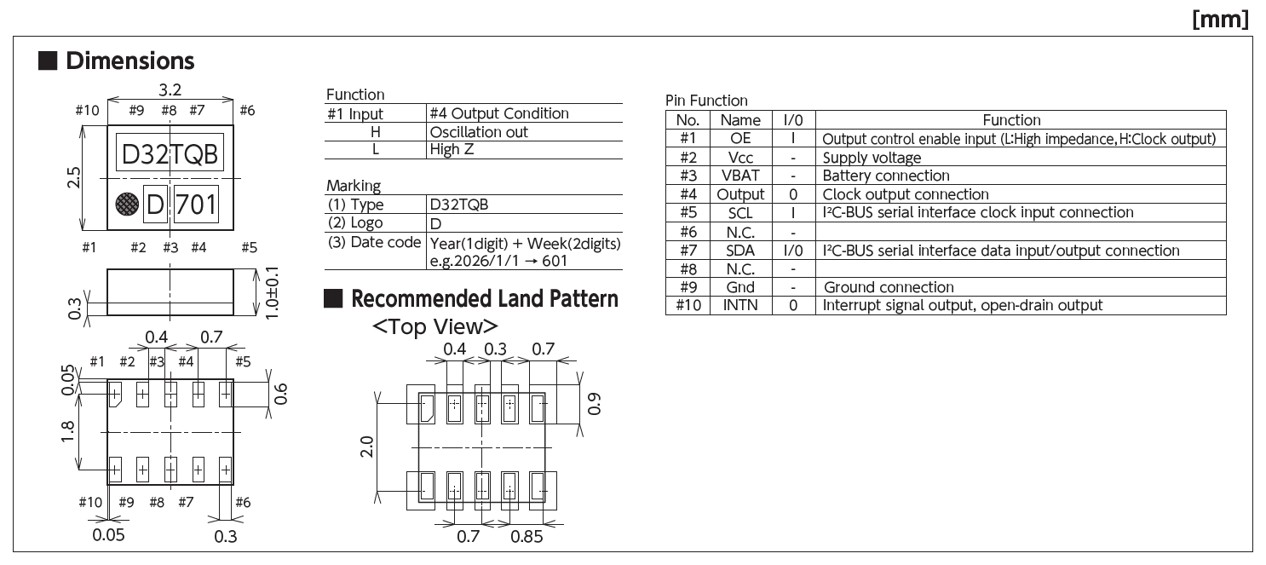
端子说明
| No. | Name | I/O | Function |
|---|---|---|---|
| #1 | OE | I | Output control enable input (L: High impedance,H: Clock output) |
| #2 | VCC | - | Supply voltage |
| #3 | VBAT | - | Battery connection |
| #4 | Output | O | Clock output connection |
| #5 | SCL | I | I2C-BUS serial interface clock input connection |
| #6 | N.C. | - | CMOS output for internal status output |
| #7 | SDA | I/O | I2C-BUS serial interface data input/output connection |
| #8 | N.C. | - | |
| #9 | GND | - | Ground connection |
| #10 | INTN | O | Interrupt signal output, open-drain output |
外形尺寸等 (点击看大图)
参考
TEL:+81-79-425-3141
FAX:+81-79-425-1134
FAX:+81-79-425-1134