Commercialization of the world’s smallest and thinnest crystal timing device with a product thickness of 1/2 or less than conventional products
DAISHINKU CORP. (President: Sohei Hasegawa) is pleased to announce that we have commercialized a crystal timing device “Arch.3G” series with a remarkably reduced thinness by a structure that differs from conventional products. This series adopts a new structure different from conventional products using a conductive adhesive, ceramic package and lid materials in order to make the device smaller, thinner and with greater reliability.
With the Arch.3G series, both the resonator and oscillator realize the world’s thinnest thickness of 1/2 or less in comparison with conventional structures. This thinness enables us to propose new value that will contribute to space saving for molded SiP (system in package) modules in which this product is stacked on silicon die and embedded in a substrate, etc.
This series is currently available as a sample, and mass production is scheduled to start in May 2018.
* Source: survey by DAISHINKU CORP. valid as of June 12, 2017
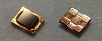 DS1008J
| Series name | Arch.3G |
| Applications | Smartphones, IoT/wearable devices, automotive, embedded in IC/SiP |
| Production Base | Tottori Production Div./Tokushima Production Div. |
| Resonators | Oscillators | |||
|---|---|---|---|---|
| SPXO | TCXO | |||
| Type | DX1008J | DX0806J | DS1008J | DB1008J |
| Size | 1.0×0.8mm | 0.8×0.6mm | 1.0×0.8mm | 1.0×0.8mm |
| Height (typ.) | 0.13mm | 0.13mm | 0.23mm | 0.23mm |
| Mass production date | May, 2018 | Undecided | May, 2018 | May, 2018 |
With conventional structures, the smaller the product the more difficult it is to secure margins for application accuracy of a conductive adhesive and mounting position when crystal elements are mounted in a package. In order to solve this issue, it was necessary to fundamentally review product and process designs.
By using our independently developed bonding technique Fine Seal technology, this series has realized hermeticity equal to that of conventional structures by making WLP (Wafer Level Package) in which 3 layer wafers using crystal as a base are attached. With a monolithic structure, this makes it possible to integrate the holding part and resonating part without a conductive adhesive and solves process problems described above, and at the same time, it significantly improves impact resistance. Furthermore, quality risks are remarkably reduced by performing wafer cleaning to bonding under a vacuum atmosphere. With these advancements, we will continue to contribute to automotive applications that require ever-increasing reliability including automatic operation.
In addition, as crystal elements of the AT cut crystal resonator have become thinner in connection with higher frequency, problems have occurred with quality and productivity arising from the process. On the other hand, handling of the Arch.3G series has become easier throughout the production process with the adoption of WLP, and these problems have been resolved. From hereon, we will focus our efforts on introduction of this product in response to Wi-Fi markets that require higher frequencies in association with increases in speed and capacitance, and information network-related products that are expected to expand in number, corresponding to 200MHz fundamental waves.
Furthermore, realization of remarkable thinness allows us to offer incredible value that assumes new mounting application scenes for crystal devices such as embedding in SiP modules that are expected to expand and IC packages. Also, this product can flexibly respond to package terminal designs and it is now possible to form various terminals such as shapes for wire-bonding.
[Comparison with conventional products]
~Resonators~

~Oscillators~

[Electrical specification]
| Type | DS1008J |
|---|---|
| Size | 1.0 × 0.8 × 0.23 mm Typ. |
| Output Frequency Range | 1 ~ 100 MHz |
| Supply Voltage | 1.6 ~ 3.6 V |
| Current Consumption | 1.3mA (Vcc = 1.8V, 48MHz), 2.0mA (Vcc = 1.8V, 96MHz) |
| Frequency Tolerance | ±20×10-6, ±30×10-6, ±50×10-6, ±100×10-6 |
| Operating Temperature Range | - 40 ~ + 85℃ |
| Output Specification | CMOS |
| Storage Temperature Range | - 40 ~ +85℃ |
| Packing Unit | 3000pcs. / reel(φ180) |
Consult our sales representative for other specifications.
[Dimensions]

- Uploaded "KDS New Wave" [Story-22] Advantages in the Manufacture of the Arkh.2G
- Financial Results Briefing for the First Half Ended September 30, 2025 (FY2026 Q2)
- Improved KDS-DAC Which Combines CO2 Capture with Hydrogen Generation
- Updated "IC Manufacturer Information"
- Notice Regarding SBT Certification for Its Greenhouse Gas Emissions Reduction Targets