Development of Miniature High-Precision SMD TCXO for GPS
DAISHINKU Corporation (President: Sohei Hasegawa) announces the development of the DSB321SDA/ DSB221SDA, a Miniature High-Precision Temperature Compensated Crystal Oscillator (TCXO), for GPS related applications. Samples of the DSB321SDA/DSB221SDA are available now. A high precision SMD TCXO is typically used in the receiver section of a GPS related product. GPS related products require a very high precision and high performance TCXO to minimize its TTFF (Time To First Fix) and to maximize performance especially in weak-signal environments.
DAISHINKU Corporation currently produces High-precision SMD TCXO, DSB321SD, which provides frequency temperature stability of +/-0.5ppm / -30C to +85C, for the GPS related products. At this time, the phase noise performance of the output signal is improved with the new TCXO (DSB321SDA/ DSB221SDA) to enhance the sensitivity of the GPS receivers with the same frequency temperature stability of +/-0.5ppm / -30C to +85C. At the same time, the available supply voltage range has also been lowered down to +1.7V ~ +3.6V to enable the GPS receivers to use the TCXO at +1.8V. This has been strongly required by the industry. The new TCXO can also be used at the existing supply voltage anywhere in the +1.7V to +3.6V range. (The available supply voltage range of the existing product: +2.3V to +5.5V)
In addition to these above features, a build-in standby function (also called an “on-off”, or “enable-disable”) is also integrated into the new TCXO as an optional function. The standby function controls the switching of the TCXO by the external standby signals. With the conventional TCXOs, the power supply to the TCXO is typically controlled by external power management ICs or external LDOs (Low dropout regulators) in the system. The new TCXO (DSB321SDA/DSB221SDA) can be easily controlled by just applying standby signal from the system. In addition, the standby function of the new TCXO is eliminating the need for the external power management circuitry and significantly simplifying the design around the TCXO with the minimum board space as well as the reduced numbers of BOM (about 4 components can be eliminated with the TCXO compare to the conventional system using the current TCXO and the LDOs)
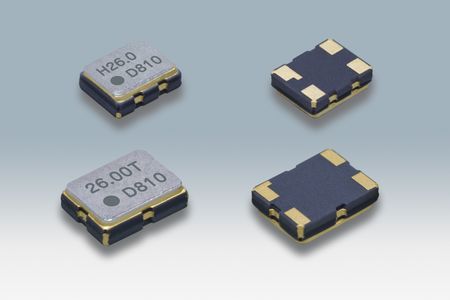
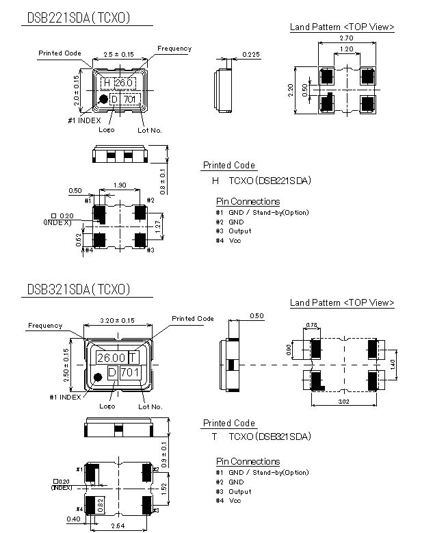
The DSB321SDA (3.2 x 2.5 x 0.9mm) and the DSB221SDA (2.5 x 2.0 x 0.8mm) were developed based on these new technologies. These products adopted the single packaged structure, as well as the existing KDS TCXO products, and enabled our manufacturing line to share the production equipment to produce the new product more flexibly and efficiently to support the expanding market need in the GPS related applications (Navigation systems, PNDs and Cell phones etc).
- [Features]
-
- Miniature and High-Precision
2520size (2.5 x 2.0 x 0.8mm, Volume 0.0045cc, Weight 0.02g)
3225size (3.2 x 2.5 x 0.9mm, Volume 0.0072cc, Weight 0.03g)
Frequency stability +/-0.5ppm / -30 degree C to +85 degree C - Low voltage Supply voltage range from +1.7V to +3.6V
- Low harmonics
Minimized harmonics (reducing the risk of interference with the carrier frequencies) - Low phase noise
-5dBc/Hz improvement from the existing TCXO
(at 16.369MHZ, Offset 10Hz) - Single packaged structure
Moisture Sensitivity Level: LEVEL 1
(IPC/JEDEC J-STD-033) - Lead-free
- Miniature and High-Precision
- [Applications]
- GPS-related equipment (navigation systems, PNDs, cell phones), GPS module
- [Sample price]
- 1,000yen
- [Mass production]
- June, 2008
- [Manufacturing Capacity ]
- 1 million/month
- [Electrical specification]
-
Item DSB221SDA (2520-size TCXO)/
DSB321SDA (3225-size TCXO)Output Frequency Range
9.6MHz to 40MHz
Output Frequency
16.3676/ 16.368/ 16.369/ 16.8/ 18.414/ 23.104/ 24.5535/ 26MHz
Supply Voltage
+1.8V +2.5V +2.8V +3.0V +3.3V
Current Consumption
(Operating Current)
+1.2 mA max. (F = 15MHz)
+1.4 mA max. (15 < F = 26MHz)
+1.6 mA max. (F > 26MHz)(Standby Current)
+1 uA and below
TCXO Output Level
0.8Vp-p min.
TCXO Output Load
(10kO//10pF) ±10%
Frequency Stability Tolerance
±1.5×10⁻⁶(After 2 reflows)
vs. Temperature
±0.5×10⁻⁶/-30°C to +85°C
±0.5×10⁻⁶/-40°C to +85°C(Option)vs. Supply Voltage
±0.2×10⁻⁶/(+1.8V±0.1V)
vs. Load Variation
±0.2×10⁻⁶/(10kO//10pF)±10%
vs. Aging
±1.0×10⁻⁶/year
Phase Noise
-94dBc/Hz typ. @10Hz/-117dBc/Hz typ. @100Hz (@ Output Frequency 16.369MHz)
Start up Time
2.0msec max.
*Consult our sales representative for other specifications.
- [Outline View ]
- Financial Results Supplementary Materials for the First Three Quarters Ended December 31, 2025 (FY2026 Q3)
- Summary of Financial Results for the First Three Quarters Ended December 31, 2025
- Uploaded "KDS New Wave" [Story-22] Advantages in the Manufacture of the Arkh.2G
- Transcript of the second quarter financial results briefing for the first half ended September 30, 2025 (FY2026 Q2)
- Financial Results Briefing for the First Half Ended September 30, 2025 (FY2026 Q2)